鈥?/div>
Pb鈭扚ree Packages are Available
1
BASE
COLLECTOR
3
MAXIMUM RATINGS
Rating
Collector 鈭扙mitter Voltage
Collector 鈭払ase Voltage
Emitter 鈭払ase Voltage
Collector Current 鈭?Continuous
Symbol
V
CEO
V
CBO
V
EBO
I
C
Value
45
50
5.0
500
Unit
V
V
V
mAdc
1
2
3
2
EMITTER
Maximum ratings are those values beyond which device damage can occur.
Maximum ratings applied to the device are individual stress limit values (not
normal operating conditions) and are not valid simultaneously. If these limits
are exceeded, device functional operation is not implied, damage may occur
and reliability may be affected.
THERMAL CHARACTERISTICS
Characteristic
Total Device Dissipation FR鈭?5 Board, (Note 1)
T
A
= 25擄C
Derate above 25擄C
Thermal Resistance, Junction鈭抰o鈭扐mbient
Total Device Dissipation
Alumina Substrate, (Note 2) T
A
= 25擄C
Derate above 25擄C
Thermal Resistance, Junction鈭抰o鈭扐mbient
Junction and Storage Temperature
1. FR鈭? = 1.0 x 0.75 x 0.062 in.
2. Alumina = 0.4 x 0.3 x 0.024 in 99.5% alumina.
Symbol
P
D
225
1.8
R
qJA
P
D
300
2.4
R
qJA
T
J
, T
stg
417
鈭?5 to
+150
mW
mW/擄C
擄C/W
擄C
xx
D
556
mW
mW/擄C
擄C/W
Max
Unit
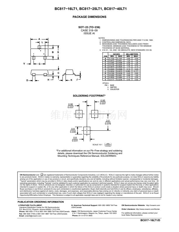
SOT鈭?3
CASE 318
STYLE 6
MARKING DIAGRAM
xxD
= Specific Device Code
= Date Code
ORDERING INFORMATION
See detailed ordering and shipping information in the package
dimensions section on page 2 of this data sheet.
漏
Semiconductor Components Industries, LLC, 2004
1
June, 2004 鈭?Rev. 6
Publication Order Number:
BC817鈭?6LT/D


 1
1
 2
2
 3
3
 4
4
