鈥?/div>
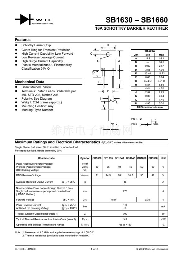
10.5
C
2.62
2.87
D
3.56
4.06
E
13.46
14.22
F
0.68
0.94
G
3.74 脴
3.91 脴
H
5.84
6.86
I
4.44
4.70
J
2.54
2.79
K
0.35
0.64
L
1.14
1.40
P
4.95
5.20
All Dimensions in mm
A
D
Mechanical Data
!
!
!
!
!
!
Case: Molded Plastic
Terminals: Plated Leads Solderable per
MIL-STD-202, Method 208
Polarity: See Diagram
Weight: 2.24 grams (approx.)
Mounting Position: Any
Marking: Type Number
F
P
I
L
H
E
PIN 1 +
+
Case
J
K
PIN 2 -
Maximum Ratings and Electrical Characteristics
Single Phase, half wave, 60Hz, resistive or inductive load.
For capacitive load, derate current by 20%.
Characteristic
Peak Repetitive Reverse Voltage
Working Peak Reverse Voltage
DC Blocking Voltage
RMS Reverse Voltage
Average Rectified Output Current
@T
C
= 95擄C
Symbol
V
RRM
V
RWM
V
R
V
R(RMS)
I
O
@T
A
=25擄C unless otherwise specified
SB1630 SB1635 SB1640 SB1645 SB1650 SB1660
30
21
35
24.5
40
28
16
45
31.5
50
35
60
42
Unit
V
V
A
Non-Repetitive Peak Forward Surge Current 8.3ms
Single half sine-wave superimposed on rated load
(JEDEC Method)
Forward Voltage
Peak Reverse Current
At Rated DC Blocking Voltage
Typical Junction Capacitance (Note 1)
Typical Thermal Resistance Junction to Case (Note 2)
Operating and Storage Temperature Range
@I
F
= 16A
@T
A
= 25擄C
@T
A
= 100擄C
I
FSM
V
FM
I
RM
C
j
R
�JC
T
j
, T
STG
0.57
275
0.75
1.0
50
700
3.5
-65 to +150
A
V
mA
pF
K/W
擄C
Note: 1. Measured at 1.0 MHz and applied reverse voltage of 4.0V D.C.
2. Thermal resistance junction to case mounted on heatsink.
SB1630 鈥?SB1660
1 of 3
漏 2002 Won-Top Electronics


 1
1
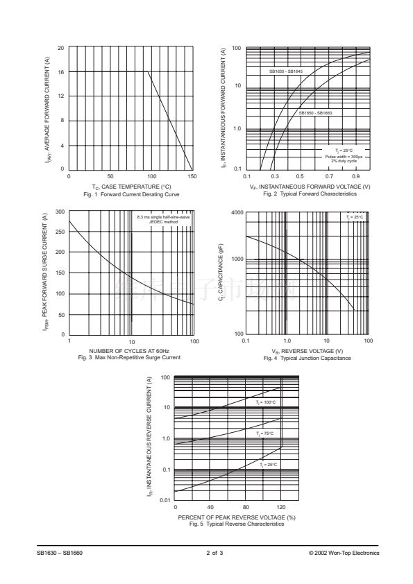 2
2
 3
3
