鈩?/div>
system,
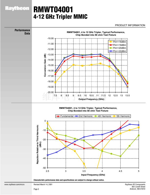
Pin = +18 dBm
Parameter
Input Frequency Range
Output Frequency Range
Input Drive Power
Conversion Loss
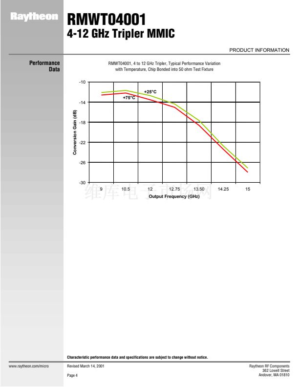
Conversion Loss Variation
vs Freq
Min
2.8
8.4
+16
Typ
Max Unit
4.0 GHz
12.0 GHz
dBm
16.5 dB
dB
Parameter
Fundamental Rejection
2nd Harmonic Rejection
4th Harmonic Rejection
5th Harmonic Rejection
Input Return Loss
(Pin = +18 dBm)
Min
Typ
-25
-20
-20
-30
10
Max Unit
dBc
dBc
dBc
dBc
dB
+18
14
0.7
Application
Information
CAUTION: THIS IS AN ESD SENSITIVE DEVICE.
Chip carrier material should be selected to have GaAs compatible thermal coefficient of expansion and high thermal
conductivity such as copper molybdenum or copper tungsten. The chip carrier should be machined, finished flat,
plated with gold over nickel and should be capable of withstanding 325擄C for 15 minutes.
Die attachment should utilize Gold/Tin (80/20) eutectic alloy solder and should avoid hydrogen environment for
PHEMT devices. Note that the backside of the chip is gold plated and is used as RF ground.
These GaAs devices should be handled with care and stored in dry nitrogen environment to prevent contamination
of bonding surfaces. These are ESD sensitive devices and should be handled with appropriate precaution including
the use of wrist grounding straps. All die attach and wire/ribbon bond equipment must be well grounded to prevent
static discharges through the device.
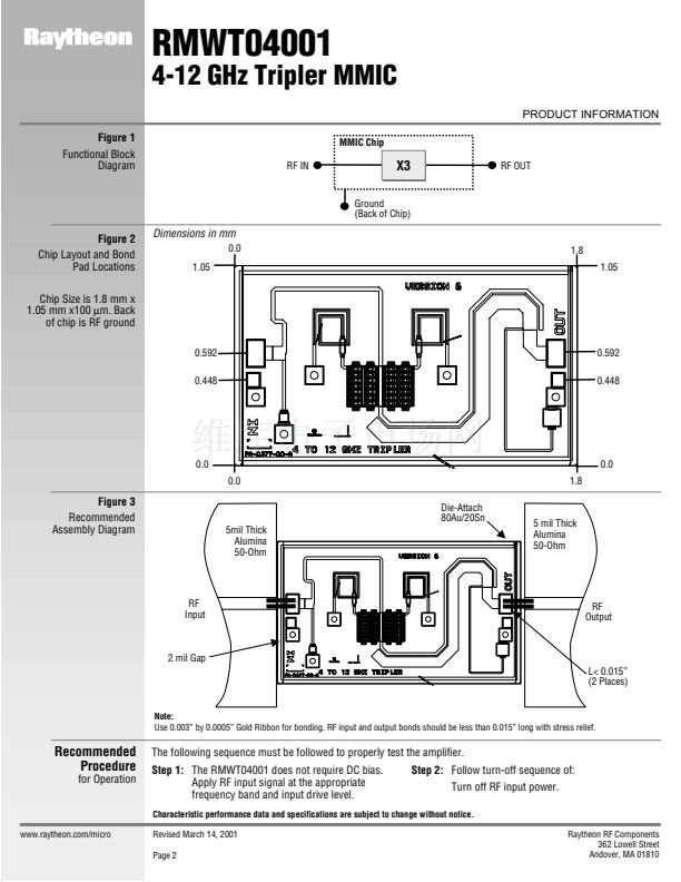
Recommended wire bonding uses 3 mils wide and 0.5 mil thick gold ribbon with lengths as short as practical
allowing for appropriate stress relief. The RF input and output bonds should be typically 0.012鈥?long corresponding
to a typically 2 mil between the chip and the substrate material.
Characteristic performance data and specifications are subject to change without notice.
www.raytheon.com/micro
Revised March 14, 2001
Page 1
Raytheon RF Components
362 Lowell Street
Andover, MA 01810


 1
1
 2
2
 3
3
 4
4
 5
5
