-
-

- 手機(jī)版
-

- 芯視頻 APP
-

- 微信公眾號(hào)
-

- 維庫(kù)官方抖音
-

- 微信頭條號(hào)
-
- |
-
- |
- |
- |

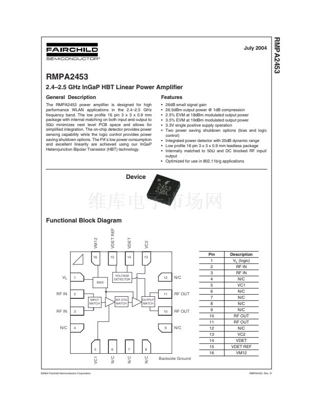
RMPA2453
2.4?2.5 GHz InGaP HBT Linear Power Amplifier
10頁(yè)
FAIRCHILD
掃碼查看芯片數(shù)據(jù)手冊(cè)
上傳產(chǎn)品規(guī)格書
4,000
RF/IF 和 RFID
RF 放大器
-
2.4GHz ~ 2.5GHz
-
24.5dB ~ 29dB
-
802.11/Wi-Fi,WLAN
3 V ~ 3.7 V
160mA ~ 200mA
-
16-LCC
帶卷 (TR)
RMPA2453TR


聯(lián)系人:
聯(lián)系方式:

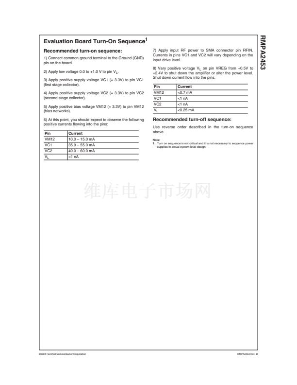
 1
1
 2
2
 3
3
 4
4
 5
5
 6
6
 7
7
 8
8
 9
9
 10
10
