1980 MHz bands. The 2 stage PAM is internally matched to
鈩?/div>
to minimize the use of external components and
features a low-power mode to reduce standby current and
DC power consumption during peak phone usage. High
power-added efficiency and excellent linearity are achieved
using Fairchild鈥檚 InGaP/GaAs Heterojunction Bipolar
Transistor (HBT) process.
Features
鈥?Single positive-supply operation and low power and
shutdown modes
鈥?42% WCDMA efficiency at +28 dBm average output
power 1920鈥?980 MHz
鈥?39% WCDMA efficiency at 27.5 dBm average output
power 1850鈥?910 MHz
鈥?Meets UMTS/WCDMA performance requirements in
both UMTS bands
鈥?Compact, low-profile package鈥?3.0 x 3.0 x 1.0 mm
nominal)
鈥?Internally matched to 50
鈩?/div>
and DC blocked RF input/
output
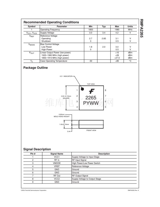
Device (3 x 3 x 1mm)
PY 226
WW5
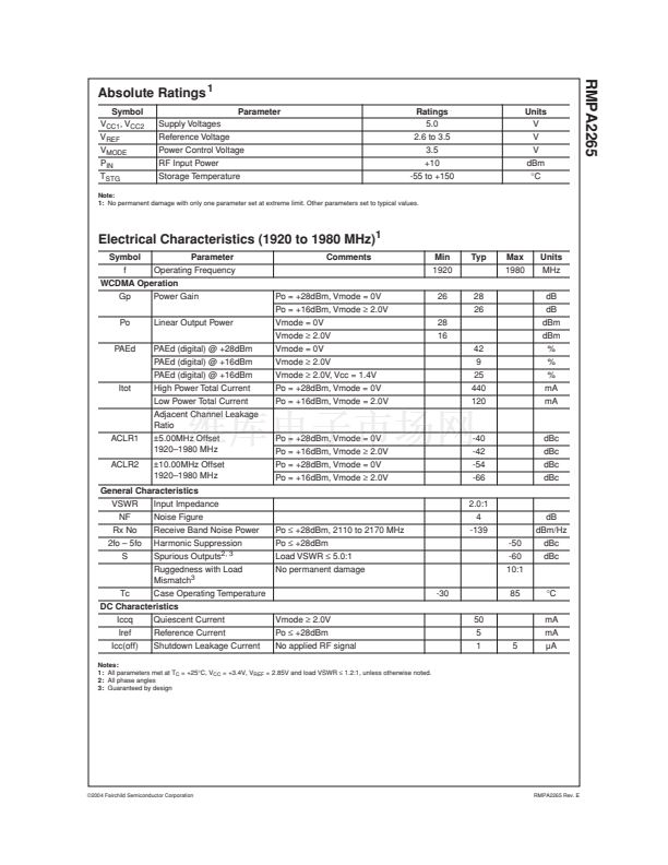
Functional Block Diagram
(Top View)
PA MODULE
MMIC
Vcc1
1
Input
Match
8
Output
Match
Vcc2
RF IN
2
7
RF OUT
Vmode
3
DC Bias Control
6
GND
Vref
4
5
GND
(paddle ground on package bottom)
漏2004 Fairchild Semiconductor Corporation
RMPA2265 Rev.
E


 1
1
 2
2
 3
3
 4
4
 5
5
 6
6
 7
7
 8
8
 9
9
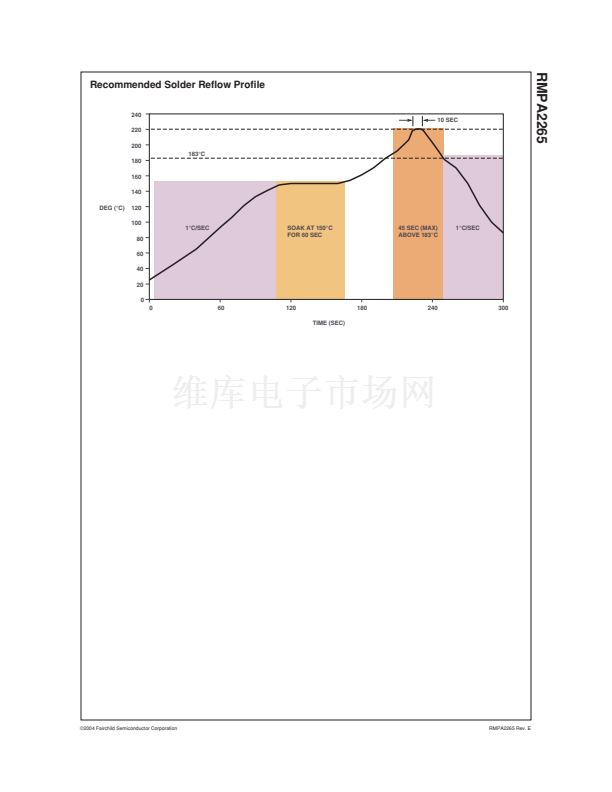 10
10
 11
11
