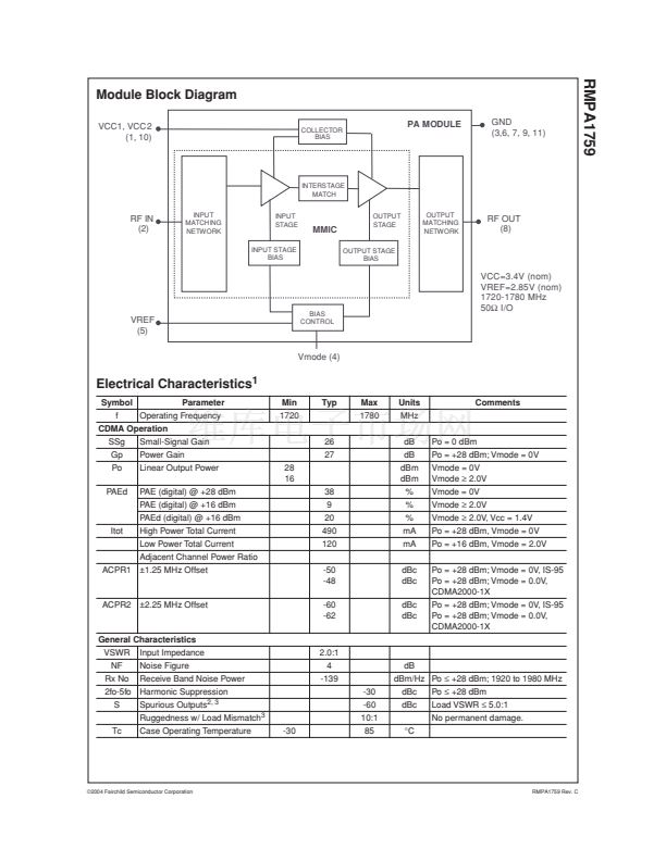
communications system (PCS) applications. The 2 stage
鈩?/div>
to minimize the use of
external components and features a low-power mode to
reduce standby current and DC power consumption during
peak phone usage. High power-added efficiency and
excellent linearity are achieved using our InGaP
Heterojunction Bipolar Transistor (HBT) process.
Features
鈥?Single positive-supply operation and low power and
shutdown modes
鈥?38% CDMA efficiency at +28dBm average output power
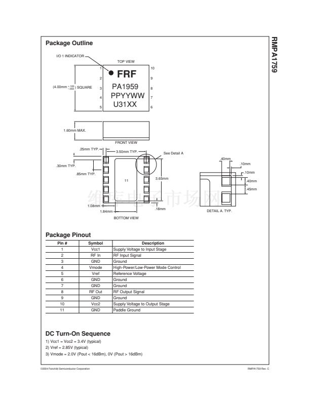
鈥?Compact LCC package- 4.0 x 4.0 x 1.5 mm with industry
standard pinout
鈥?Internally matched to 50
鈩?/div>
and DC blocked RF input/
output.
鈥?Meets CDMA2000-1XRTT performance requirements
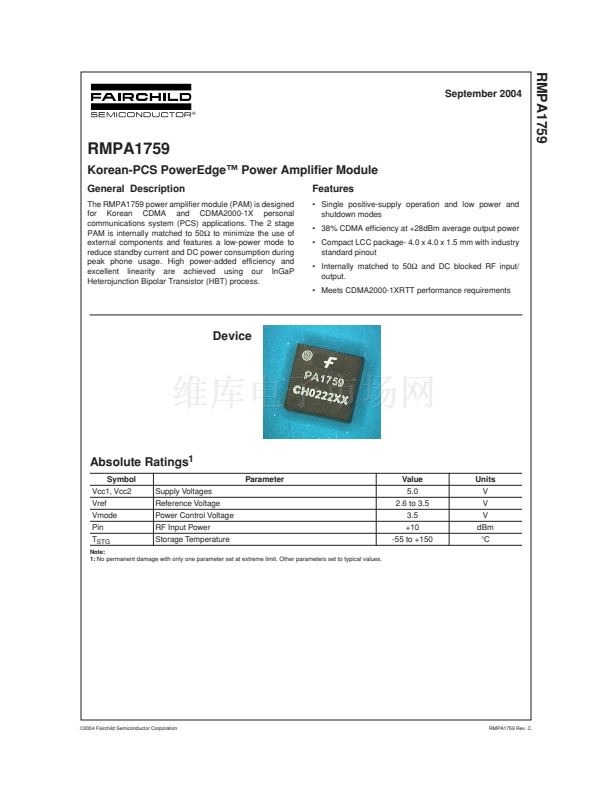
Device
Absolute Ratings
1
Symbol
Vcc1, Vcc2
Vref
Vmode
Pin
T
STG
Parameter
Supply Voltages
Reference Voltage
Power Control Voltage
RF Input Power
Storage Temperature
Value
5.0
2.6 to 3.5
3.5
+10
-55 to +150
Units
V
V
V
dBm
擄C
Note:
1:
No permanent damage with only one parameter set at extreme limit. Other parameters set to typical values.
漏2004 Fairchild Semiconductor Corporation
RMPA1759 Rev. C


 1
1
 2
2
 3
3
 4
4
 5
5
 6
6
 7
7
 8
8
