鈩?/div>
source)
Drain Current
Case Operating Temperature
Storage Temperature Range
Soldering Temperature
Symbol
Vdd
Pin(CW)
Idd
Tc
Tstg
Tsolder
Value
6.5
0
130
-35 to 85
-40 to 110
220
Unit
V
dBm
mA
擄C
擄C
擄C
Electrical
Characteristics
2
Parameter
Min
Typ
19.0
-0.008
1.4
1.5
10.0
Max
6.5
Unit
GHz
dB
dB/擄C
dB
dB
dBm
Parameter
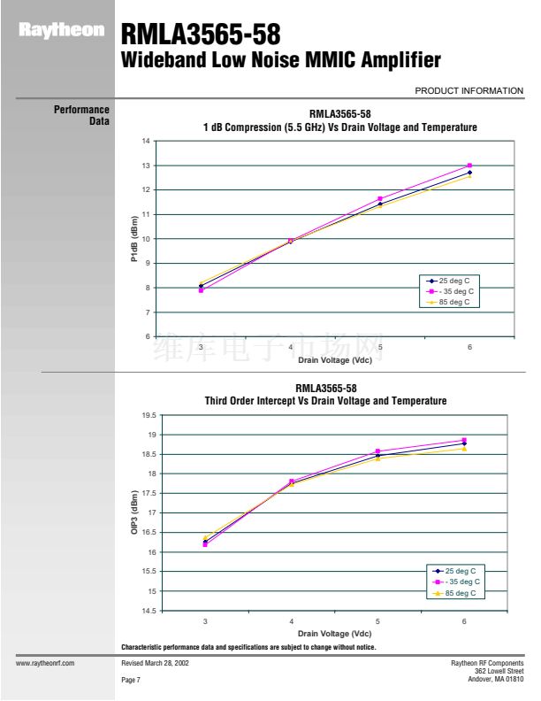
OIP3 @ 5.5 GHz, +3 dBm
Pout total
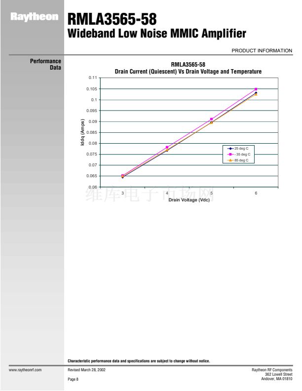
Idd
Vdd
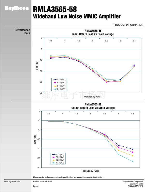
Input Return Loss
Output Return Loss
Thermal Resistance Rjc
(Channel to Case)
Min
17
3.0
Typ
21.0
70.0
4.0
-15.0
-10.0
135
Max
Unit
dBm
mA
V
dB
dB
擄C/W
Frequency Range
3.5
3,4
17.0
Gain (Small Signal)
Gain Variation vs Temp
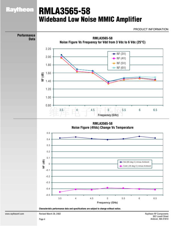
Noise Figure
4
3.5 - 5 GHz
5 - 6.5 GHz
Power Out, P1dB @ 5.5 GHz 8.0
85.0
6.0
2.2
1.6
Notes:
1. No permanent damage with only one parameter set at maximum limit and all other parameters at typical conditions
2. All parameters met at Tc = +25 擄C, Vdd = 4.0V
3. Pin = -20 dBm, Vdd = 4.0 V, Frequency 3.5 - 6.5 GHz
4. Data de-embedded from fixture loss
Characteristic performance data and specifications are subject to change without notice.
www.raytheonrf.com
Revised March 28, 2002
Page 1
Raytheon RF Components
362 Lowell Street
Andover, MA 01810


 1
1
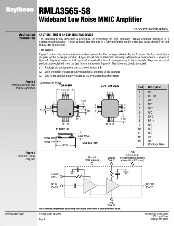 2
2
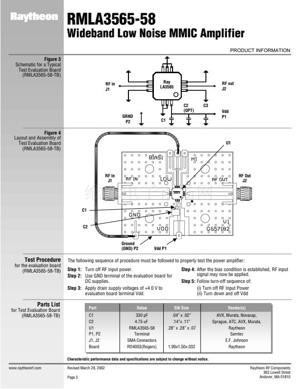 3
3
 4
4
 5
5
 6
6
 7
7
 8
8
