鈾?/div>
High temperature soldering guaranteed:
260擄C/10 seconds at 5 lbs. (2.3kg) tension
0-8
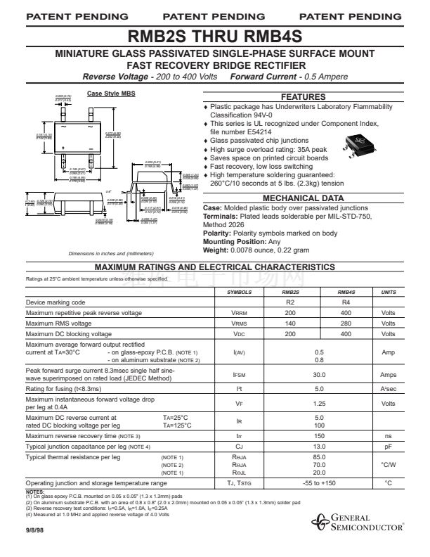
4 (2.90) 0.106 (2.70)
4 (2.40) 0.090 (2.30)
0.038 (0.96)
0.019 (0.48)
MECHANICAL DATA
Case:
Molded plastic body over passivated junctions
Terminals:
Plated leads solderable per MIL-STD-750,
Method 2026
Polarity:
Polarity symbols marked on body
Mounting Position:
Any
Weight:
0.0078 ounce, 0.22 gram
Dimensions in inches and (millimeters)
MAXIMUM RATINGS AND ELECTRICAL CHARACTERISTICS
Ratings at 25擄C ambient temperature unless otherwise specified.
SYMBOLS
RMB2S
RMB4S
UNITS
Device marking code
Maximum repetitive peak reverse voltage
Maximum RMS voltage
Maximum DC blocking voltage
Maximum average forward output rectified
- on glass-epoxy P.C.B.
(NOTE 1)
current at T
A
=30擄C
- on aluminum substrate
(NOTE 2)
Peak forward surge current 8.3msec single half sine-
wave superimposed on rated load (JEDEC Method)
Rating for fusing (t<8.3ms)
Maximum instantaneous forward voltage drop
per leg at 0.4A
Maximum DC reverse current at
rated DC blocking voltage per leg
Maximum reverse recovery time
(NOTE 3)
(NOTE 4)
(NOTE 1)
(NOTE 2)
(NOTE 1)
R2
V
RRM
V
RMS
V
DC
I
(AV)
200
140
200
0.5
0.8
30.0
5.0
1.25
5.0
100
150
13.0
85.0
70.0
20.0
-55 to +150
R4
400
280
400
Volts
Volts
Volts
Amp
I
FSM
I
2
t
V
F
Amps
A
2
sec
Volts
T
A
=25擄C
T
A
=125擄C
I
R
t
rr
C
J
R
螛JA
R
螛JA
R
螛JL
T
J
, T
STG
ns
pF
擄C/W
擄C
Typical junction capacitance per leg
Typical thermal resistance per leg
Operating junction and storage temperature range
NOTES:
(1) On glass epoxy P.C.B. mounted on 0.05 x 0.05" (1.3 x 1.3mm) pads
(2) On aluminum substrate P.C.B. with an area of 0.8 x 0.8" (2.0 x 2.0mm) mounted on 0.05 x 0.05鈥?(1.3 x 1.3mm) solder pad
(3) Reverse recovery test conditions: I
F
=0.5A, I
R
=1.0A, I
rr
=0.25A
(4) Measured at 1.0 MHz and applied reverse voltage of 4.0 Volts
9/8/98


 1
1
 2
2
