= 6.0鈩?/div>
Built in Current Limit I
LIMIT
0.140 to 0.210A at 150
o
C
Built in Voltage Clamp
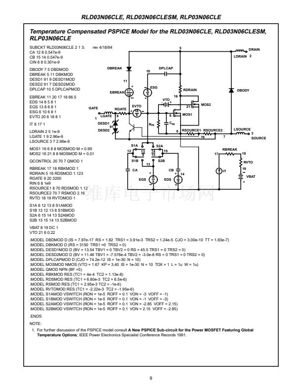
Temperature Compensating
PSPICE Model
2kV ESD Protected
Controlled Switching Limits EMI and RFI
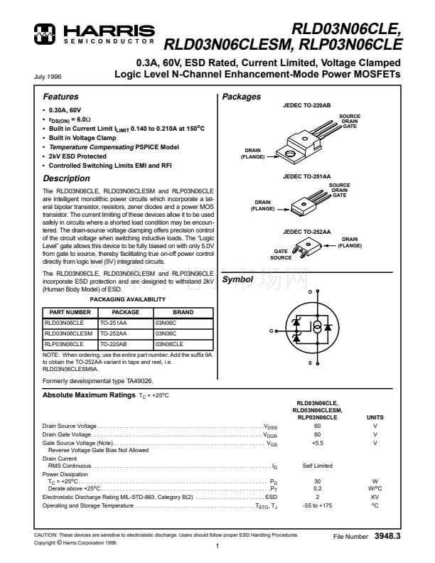
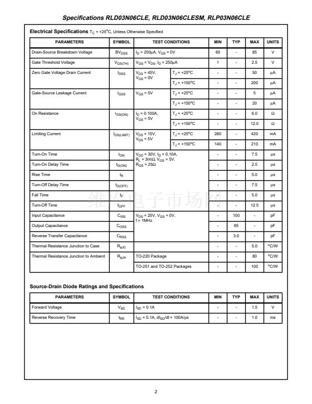
DRAIN
(FLANGE)
Description
The RLD03N06CLE, RLD03N06CLESM and RLP03N06CLE
are intelligent monolithic power circuits which incorporate a lat-
eral bipolar transistor, resistors, zener diodes and a power MOS
transistor. The current limiting of these devices allow it to be used
safely in circuits where a shorted load condition may be encoun-
tered. The drain-source voltage clamping offers precision control
of the circuit voltage when switching inductive loads. The 鈥淟ogic
Level鈥?gate allows this device to be fully biased on with only 5.0V
from gate to source, thereby facilitating true on-off power control
directly from logic level (5V) integrated circuits.
The RLD03N06CLE, RLD03N06CLESM and RLP03N06CLE
incorporate ESD protection and are designed to withstand 2kV
(Human Body Model) of ESD.
PACKAGING AVAILABILITY
PART NUMBER
RLD03N06CLE
RLD03N06CLESM
RLP03N06CLE
PACKAGE
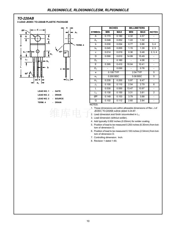
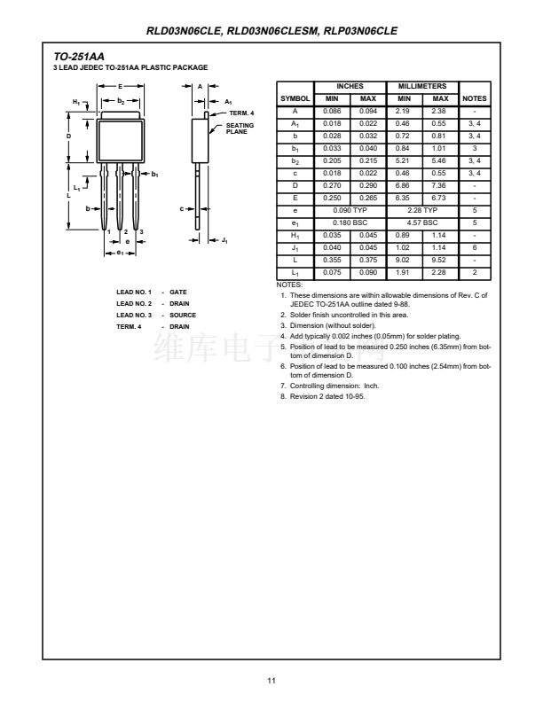
TO-251AA
TO-252AA
TO-220AB
BRAND
03N06C
03N06C
03N06CLE
G
DRAIN
(FLANGE)
JEDEC TO-251AA
SOURCE
DRAIN
GATE
JEDEC TO-252AA
DRAIN
(FLANGE)
GATE
SOURCE
Symbol
D
NOTE: When ordering, use the entire part number. Add the suf鏗亁 9A
to obtain the TO-252AA variant in tape and reel, i.e.
RLD03N06CLESM9A.
S
Formerly developmental type TA49026.
Absolute Maximum Ratings
T
C
= +25
o
C
RLD03N06CLE,
RLD03N06CLESM,
RLP03N06CLE
60
60
+5.5
Drain Source Voltage . . . . . . . . . . . . . . . . . . . . . . . . . . . . . . . . . . . . . . . . . . . . . . . . . . . . .V
DSS
Drain Gate Voltage . . . . . . . . . . . . . . . . . . . . . . . . . . . . . . . . . . . . . . . . . . . . . . . . . . . . . . V
DGR
Gate Source Voltage (Note) . . . . . . . . . . . . . . . . . . . . . . . . . . . . . . . . . . . . . . . . . . . . . . . . V
GS
Reverse Voltage Gate Bias Not Allowed
Drain Current
RMS Continuous. . . . . . . . . . . . . . . . . . . . . . . . . . . . . . . . . . . . . . . . . . . . . . . . . . . . . . . . . I
D
Power Dissipation
T
C
= +25
o
C . . . . . . . . . . . . . . . . . . . . . . . . . . . . . . . . . . . . . . . . . . . . . . . . . . . . . . . . . . . . P
D
Derate above +25
o
C . . . . . . . . . . . . . . . . . . . . . . . . . . . . . . . . . . . . . . . . . . . . . . . . . . . . . .P
T
Electrostatic Discharge Rating MIL-STD-883, Category B(2) . . . . . . . . . . . . . . . . . . . . . . ESD
Operating and Storage Temperature . . . . . . . . . . . . . . . . . . . . . . . . . . . . . . . . . . . . . . T
STG
, T
J
UNITS
V
V
V
Self Limited
30
0.2
2
-55 to +175
W
W/
o
C
KV
o
C
CAUTION: These devices are sensitive to electrostatic discharge. Users should follow proper ESD Handling Procedures.
Copyright
漏
Harris Corporation 1996
File Number
3948.3
1


 1
1
 2
2
 3
3
 4
4
 5
5
 6
6
 7
7
 8
8
 9
9
 10
10
 11
11
 12
12
 13
13
