鈾?/div>
High temperature soldering guaranteed:
450擄C/5 seconds at terminals. Complete device
submersible temperature of 260擄C for 10 seconds in
solder bath
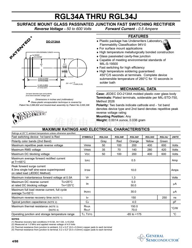
DO-213AA
E
N
T
P
A
T
SOLDERABLE ENDS
1st BAND
2nd BAND
D2
D1=
0.066
0.060
(1.676)
(1.524)
0.022 (0.559)
0.016 (0.406)
0.145 (3.683)
0.131(3.327)
1st band denotes type and polarity
2cnd band denotes voltage type
D2 = D1 + 0
- 0.008 (0.20)
MECHANICAL DATA
Case:
JEDEC DO-213AA molded plastic over glass body
Terminals:
Plated terminals, solderable per MIL-STD-750,
Method 2026
Polarity:
Two bands indicate cathode end - 1st band
denotes device type and 2nd band denotes repetitive peak
reverse voltage rating
Mounting Position:
Any
Weight:
0.0014 ounce, 0.036 gram
*
Glass-plastic encapsulation technique is covered by
Patent No.3,996,602 and brazed-lead assembly by Patent No.3,930,306
廬
Dimensions in inches and (millimeters)
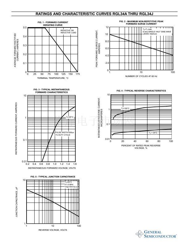
MAXIMUM RATINGS AND ELECTRICAL CHARACTERISTICS
Ratings at 25擄擄C ambient temperature unless otherwise specified.
Fast switching device: 1st band is Red
Polarity color bands (2nd Band)
Maximum repetitive peak reverse voltage
Maximum RMS voltage
Maximum DC blocking voltage
Maximum average forward rectified current
at T
T
=55擄C
Peak forward surge current
8.3ms single half sine-wave superimposed
on rated load (JEDEC Method)
Maximum instantaneous forward voltage at 0.5A
Maximum DC reverse current
at rated DC blocking voltage
T
A
=25擄C
T
A
=125擄C
SYMBOLS
RGL34A
RGL34B
RGL34D
RGL34G
RGL34J
UNITS
V
RRM
V
RMS
V
DC
I
(AV)
Gray
50
35
50
Red
100
70
100
Orange
200
140
200
0.5
Yellow
400
280
400
Green
600
420
600
Volts
Volts
Volts
Amp
I
FSM
V
F
I
R
I
R(AV)
t
rr
C
J
R
螛JA
R
螛JT
T
J
, T
STG
10.0
1.3
5.0
50.0
30.0
150
4.0
150.0
70.0
-65 to +175
250
Amps
Volts
碌A(chǔ)
碌A(chǔ)
ns
pF
擄C/W
擄C
Maximum full load reverse current, full cycle
average T
A
=55擄C
Maximum reverse recovery time
Maximum thermal resistance
(NOTE 1)
Typical junction capacitance
(NOTE 2)
(NOTE 3)
(
NOTE 4)
Operating junction and storage temperature range
NOTES:
(1) Reverse recovery test conditions I
F
=0.5A, I
R
=1.0A, I
rr
=0.25A
(2) Measured at 1.0 MHz and applied reverse voltage of 4.0 Volts
(3) Thermal resistance from junction to ambient, 0.2 x 0.2鈥?(5.0 x 5.0mm) copper pads to each terminal
(4) Thermal resistance from junction to terminal, 0.2 x 0.2鈥?(5.0 x 5.0mm) copper pads to each terminal
4/98


 1
1
 2
2
