= 0.480鈩?/div>
鈥?Very Fast Turn-Off Characteristics
鈥?Nanosecond Switching Speeds
鈥?Electrostatic Discharge Protected
鈥?UIS Rating Curve
鈥?SOA is Power Dissipation Limited
鈥?High Input Impedance
Description
The RFV10N50BE is an N-Channel fast switching MOSFET transis-
tor that is designed for switching regulators, inverters and motor driv-
ers. The RFV10N50BE is a monolithic structure incorporating a high
voltage, high current MOSFET, a control MOSFET and ESD protec-
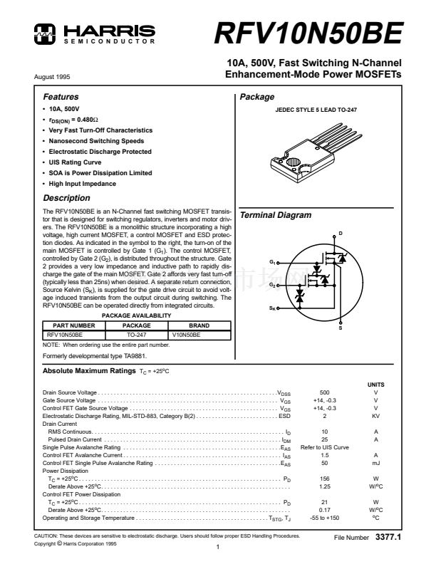
tion diodes. As indicated in the symbol to the right, the turn-on of the
main MOSFET is controlled by Gate 1 (G
1
). The control MOSFET,
controlled by Gate 2 (G
2
), is distributed throughout the structure. Gate
2 provides a very low impedance and inductive path to rapidly dis-
charge the gate of the main MOSFET. Gate 2 affords very fast turn-off
(typically less than 25ns) when desired. A separate return connection,
Source Kelvin (S
K
), is supplied for the gate drive circuit to avoid volt-
age induced transients from the output circuit during switching. The
RFV10N50BE can be operated directly from integrated circuits.
PACKAGE AVAILABILITY
PART NUMBER
RFV10N50BE
PACKAGE
TO-247
BRAND
V10N50BE
S
Terminal Diagram
D
G
1
G
2
S
K
NOTE: When ordering use the entire part number.
Formerly developmental type TA9881.
Absolute Maximum Ratings
T
C
= +25
o
C
UNITS
V
V
V
KV
A
A
A
mJ
W
W/
o
C
W
W/
o
C
o
C
Drain Source Voltage . . . . . . . . . . . . . . . . . . . . . . . . . . . . . . . . . . . . . . . . . . . . . . . . . . . . . . . . .V
DSS
Gate Source Voltage . . . . . . . . . . . . . . . . . . . . . . . . . . . . . . . . . . . . . . . . . . . . . . . . . . . . . . . . . V
GS
Control FET Gate Source Voltage . . . . . . . . . . . . . . . . . . . . . . . . . . . . . . . . . . . . . . . . . . . . . . . V
GS
Electrostatic Discharge Rating, MIL-STD-883, Category B(2) . . . . . . . . . . . . . . . . . . . . . . . . . . ESD
Drain Current
RMS Continuous. . . . . . . . . . . . . . . . . . . . . . . . . . . . . . . . . . . . . . . . . . . . . . . . . . . . . . . . . . . . . I
D
Pulsed Drain Current . . . . . . . . . . . . . . . . . . . . . . . . . . . . . . . . . . . . . . . . . . . . . . . . . . . . . . . . I
DM
Single Pulse Avalanche Rating . . . . . . . . . . . . . . . . . . . . . . . . . . . . . . . . . . . . . . . . . . . . . . . . . .E
AS
Control FET Avalanche Current . . . . . . . . . . . . . . . . . . . . . . . . . . . . . . . . . . . . . . . . . . . . . . . . . . I
AS
Control FET Single Pulse Avalanche Rating . . . . . . . . . . . . . . . . . . . . . . . . . . . . . . . . . . . . . . . .E
AS
Power Dissipation
T
C
= +25
o
C . . . . . . . . . . . . . . . . . . . . . . . . . . . . . . . . . . . . . . . . . . . . . . . . . . . . . . . . . . . . . . . . P
D
Derate Above +25
o
C. . . . . . . . . . . . . . . . . . . . . . . . . . . . . . . . . . . . . . . . . . . . . . . . . . . . . . . . . . . .
Control FET Power Dissipation
T
C
= +25
o
C . . . . . . . . . . . . . . . . . . . . . . . . . . . . . . . . . . . . . . . . . . . . . . . . . . . . . . . . . . . . . . . . P
D
Derate Above +25
o
C. . . . . . . . . . . . . . . . . . . . . . . . . . . . . . . . . . . . . . . . . . . . . . . . . . . . . . . . . . . .
Operating and Storage Temperature . . . . . . . . . . . . . . . . . . . . . . . . . . . . . . . . . . . . . . . . . . T
STG
, T
J
CAUTION: These devices are sensitive to electrostatic discharge. Users should follow proper ESD Handling Procedures.
Copyright
500
+14, -0.3
+14, -0.3
2
10
25
Refer to UIS Curve
1.5
50
156
1.25
21
0.17
-55 to +150
漏
Harris Corporation 1995
File Number
3377.1
1


 1
1
 2
2
 3
3
 4
4
 5
5
 6
6
