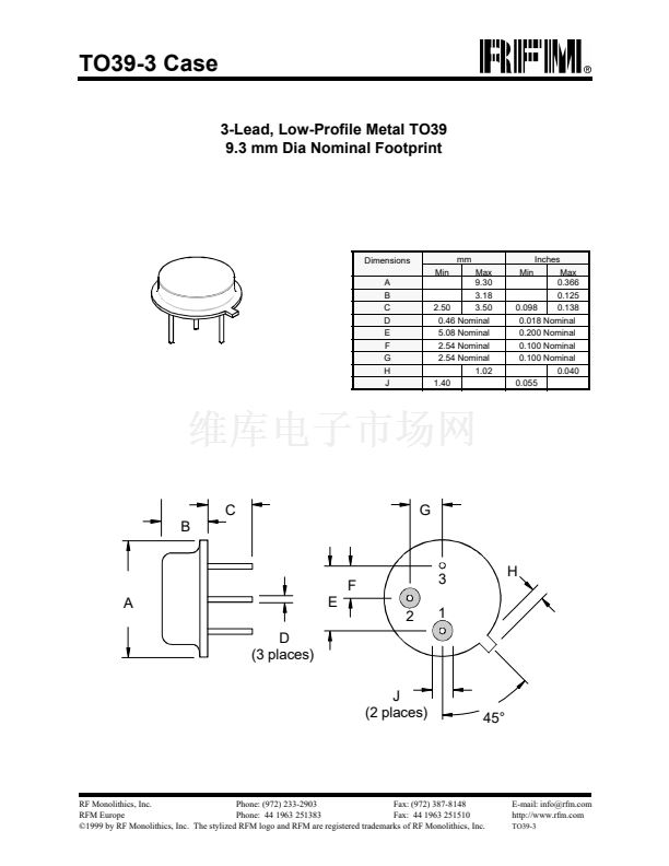
on PCB layout and external impedance matching design. See Application Note No. 42 for details. All 鈥淣C鈥?or 鈥渘o connection鈥?/div>
terminals should be grounded.
4. 鈥淟RIP鈥?or 鈥淟鈥?after the part number indicates 鈥渓ow rate initial production鈥?and 鈥淓NG鈥?or 鈥淓鈥?indicates 鈥渆ngineering prototypes.鈥?/div>
5. The design, manufacturing process, and specifications of this filter are subject to change.
6. Either Port 1 or Port 2 may be used for either input or output in the design. However, impedances and impedance matching may
vary between Port 1 and Port 2, so that the filter must always be installed in one direction per the circuit design.
7. US and international patents may apply.
8. RFM, stylized RFM logo, and RF Monolithics, Inc. are registered trademarks of RF Monolithics, Inc.
9.
漏Copyright
1999, RF Monolithics Inc.
10. Electrostatic Sensitive Device. Observe precautions for handling.
RF Monolithics, Inc.
4347 Sigma Road
Dallas, Texas 75244
USA
Phone: +1(972)233-2903
Fax: +1(972)387-8148
e-mail:
info@rfm.com
Home page:
www.rfm.com
European Sales Office
RF1046 7/22/1999 R


 1
1
 2
2
 3
3
