鈩?/div>
SC400 Microcontroller
Register Set Reference Manual
Including Changes for the 脡lanSC410 Microcontroller
This document amends the
脡lan鈩C400 Microcontroller Register Set Reference Manual
, order #21032A, including
additional information for the 脡lanSC410 microcontroller. It consists of three parts:
s
鈥淒ocumentation Defects and Corrections鈥?lists documentation defects found in the original publication.
s
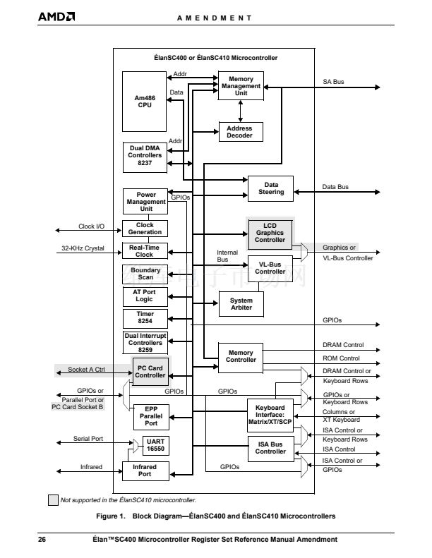
鈥淐hanges for the 脡lanSC410 Microcontroller鈥?on page 25 gives an overview of differences between the
脡lanSC400 microcontroller and the 脡lanSC410 microcontroller, and lists all the registers and bits not supported
on the 脡lanSC410 microcontroller.
s
The Index beginning on page 35 includes all of the registers listed in this document, with index offsets listed sep-
arately by subsystem.
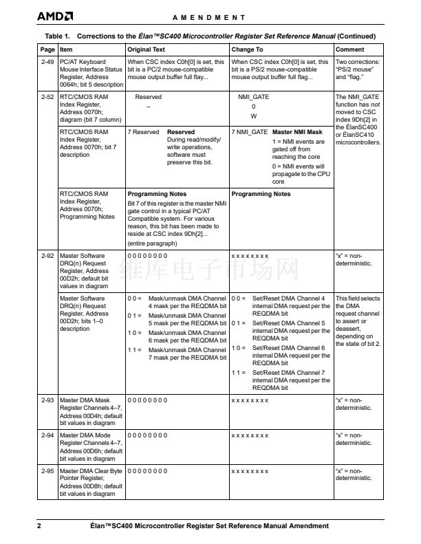
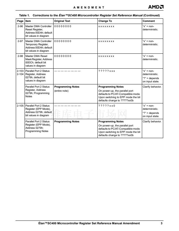
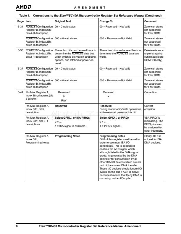
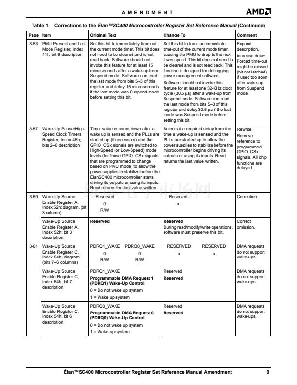
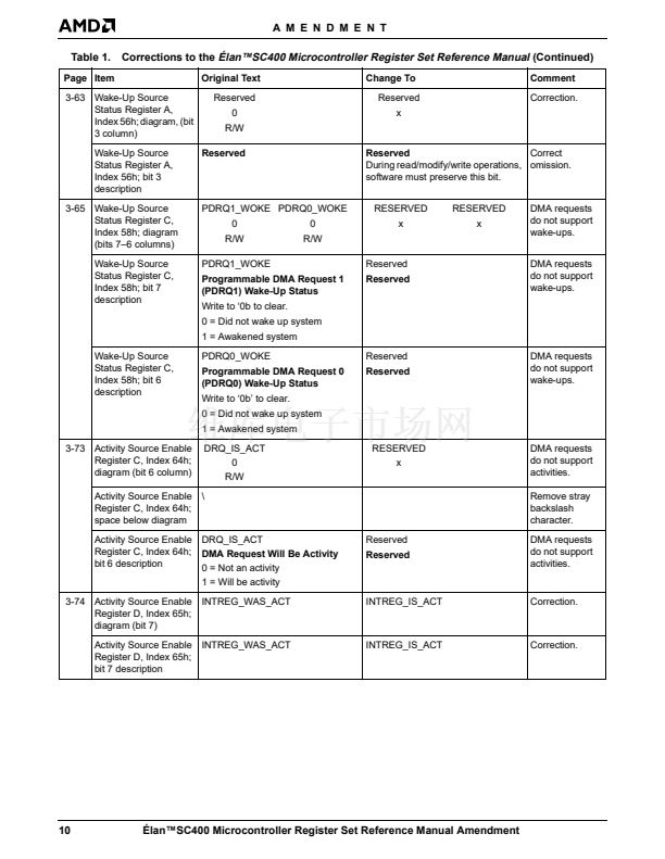
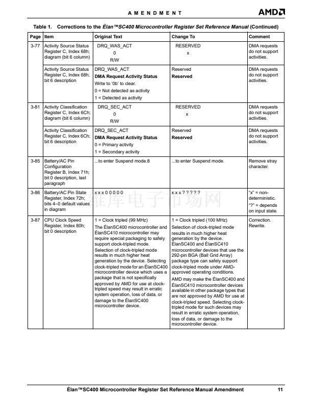
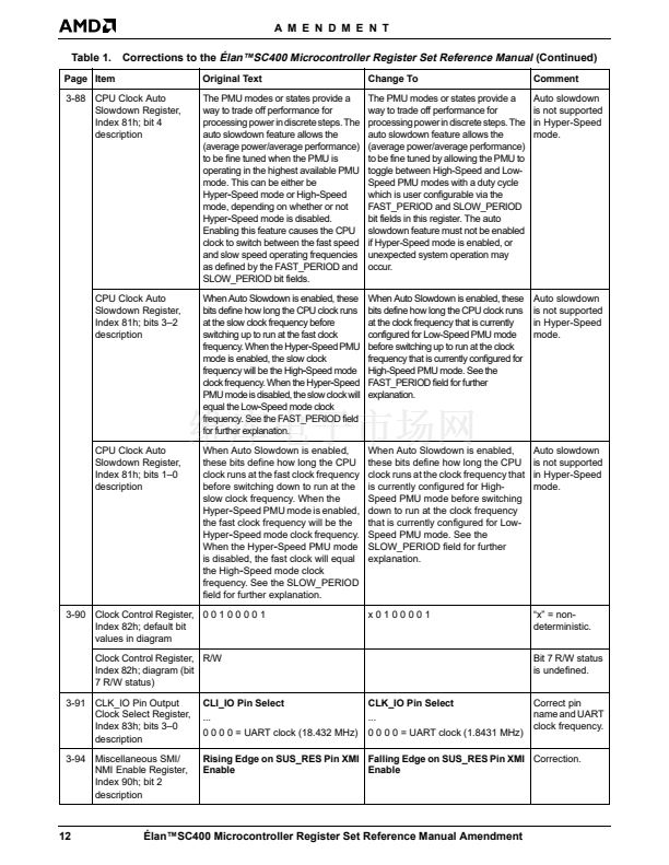
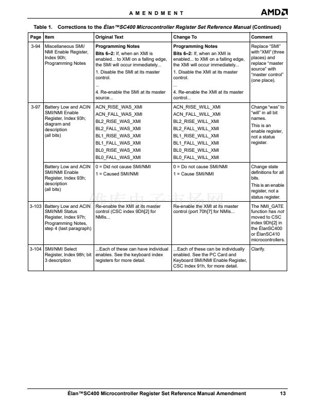
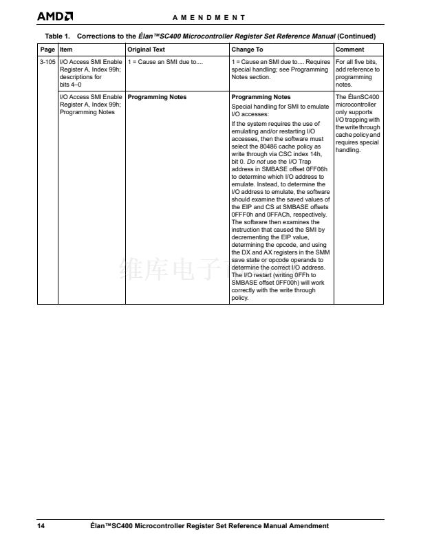
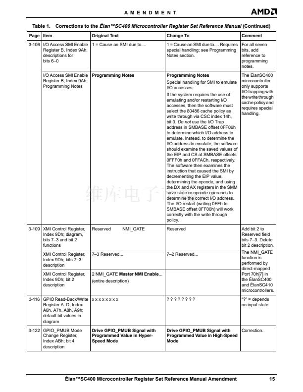
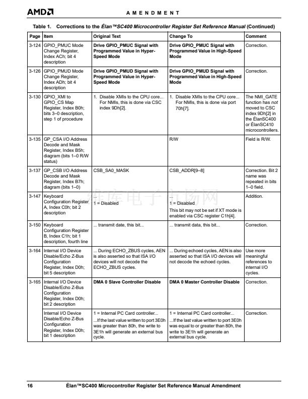
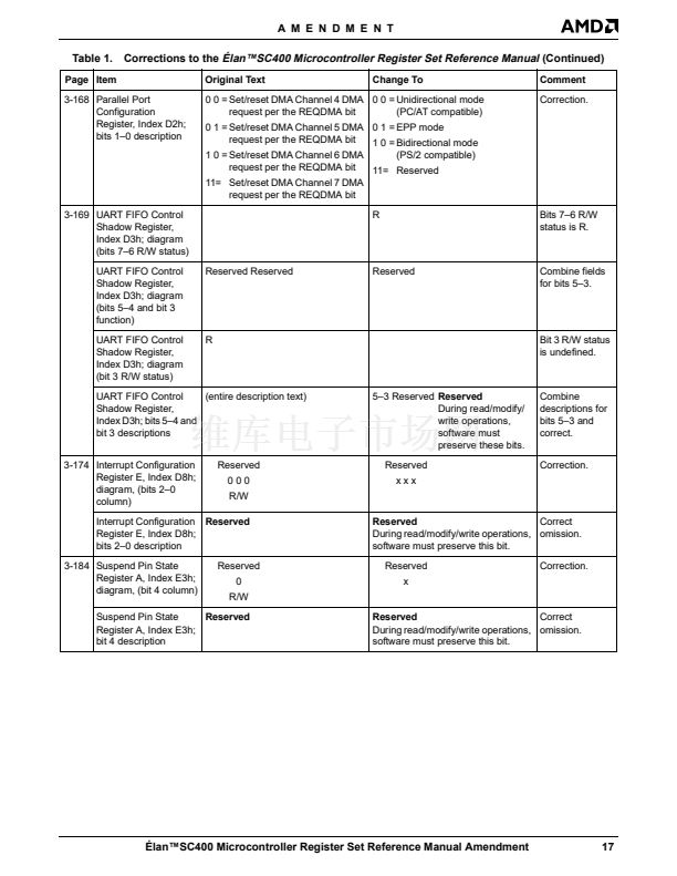
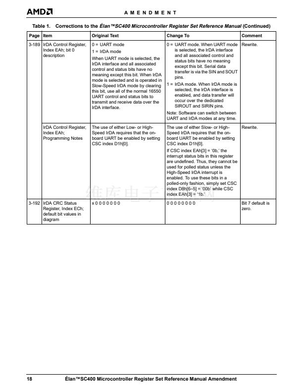
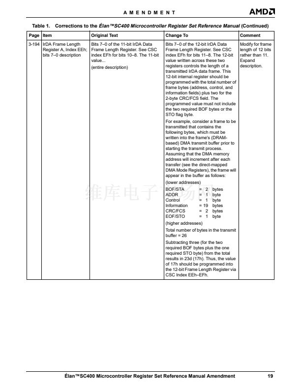
DOCUMENTATION DEFECTS AND CORRECTIONS
Table 1 lists defects that have been found in the
脡lan鈩C400 Microcontroller Register Set Reference
Manual,
order #21032A. Defects are listed in page or-
der. Each entry lists the following:
s
page number
s
item to be corrected
s
original text
s
corrected text
s
comments explaining the change
Table entries that correct text in a diagram do not con-
tain the entire diagram. If a default value is changed,
the original and changed default values are shown for
the whole register. If other text is changed, the entry de-
scribes the affected part of the diagram and lists the
original and changed text.
Each item description includes the register name, so
changes affecting a particular register can be found by
consulting the index in this document.
Unchanged portions of a paragraph are replaced by an
ellipsis (...) in entries where this might make the
change easier to find. The whole paragraph is included
if it is useful for understanding why the change was
made.
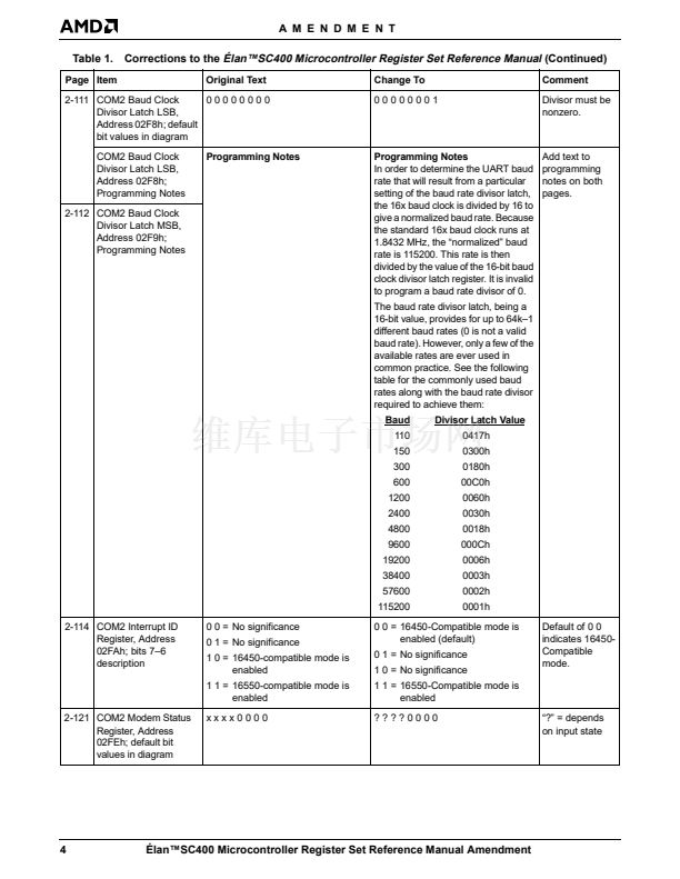
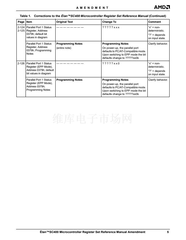
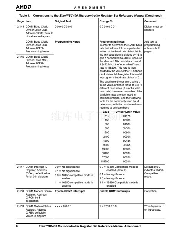
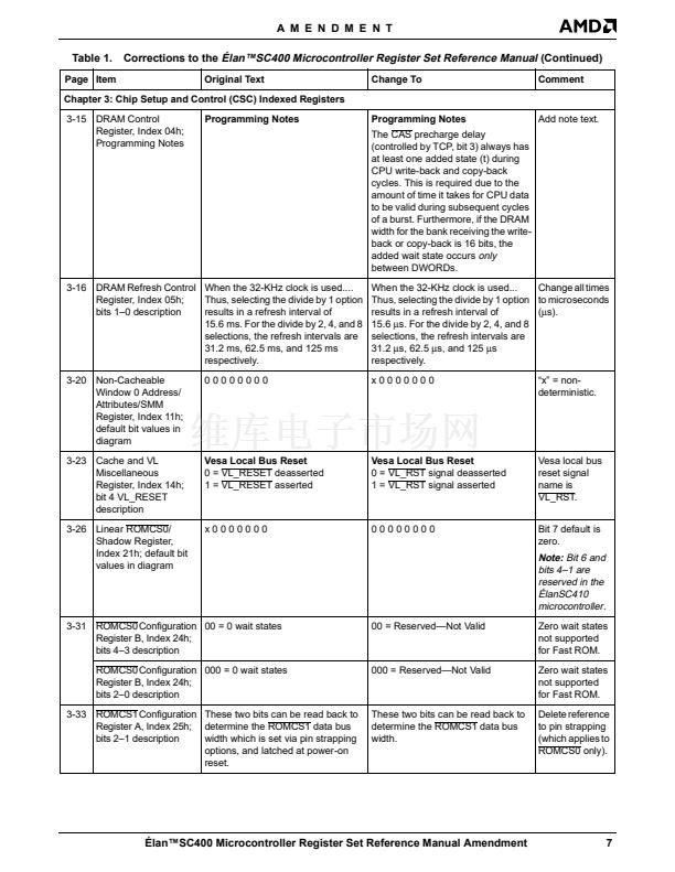
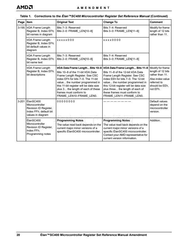
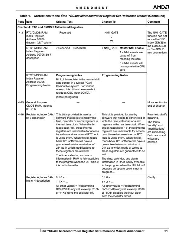
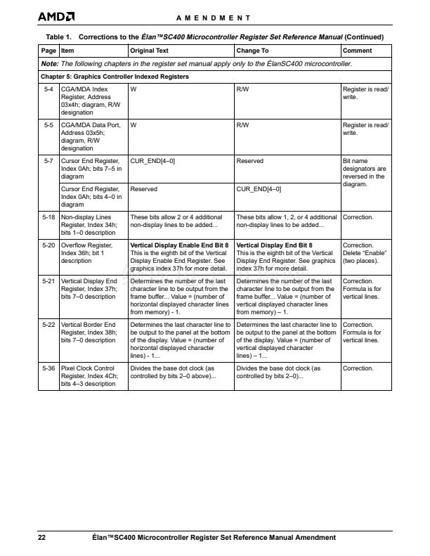
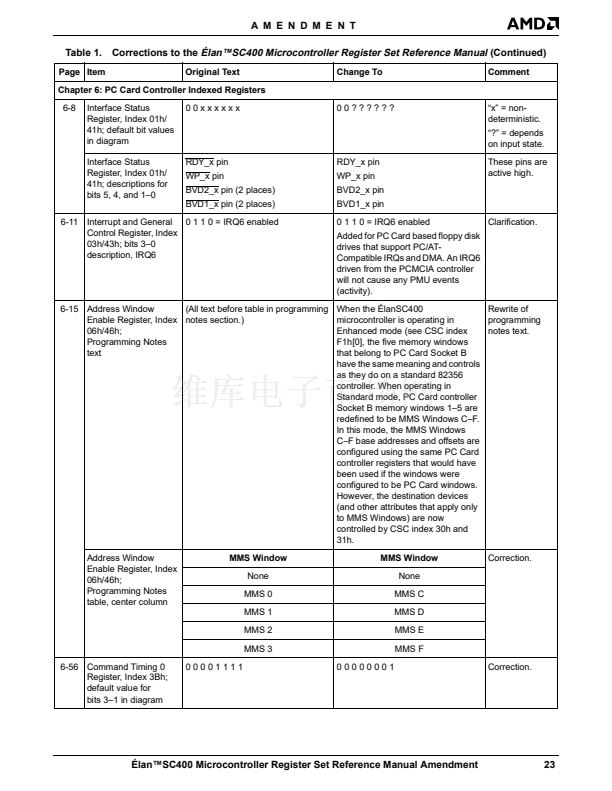
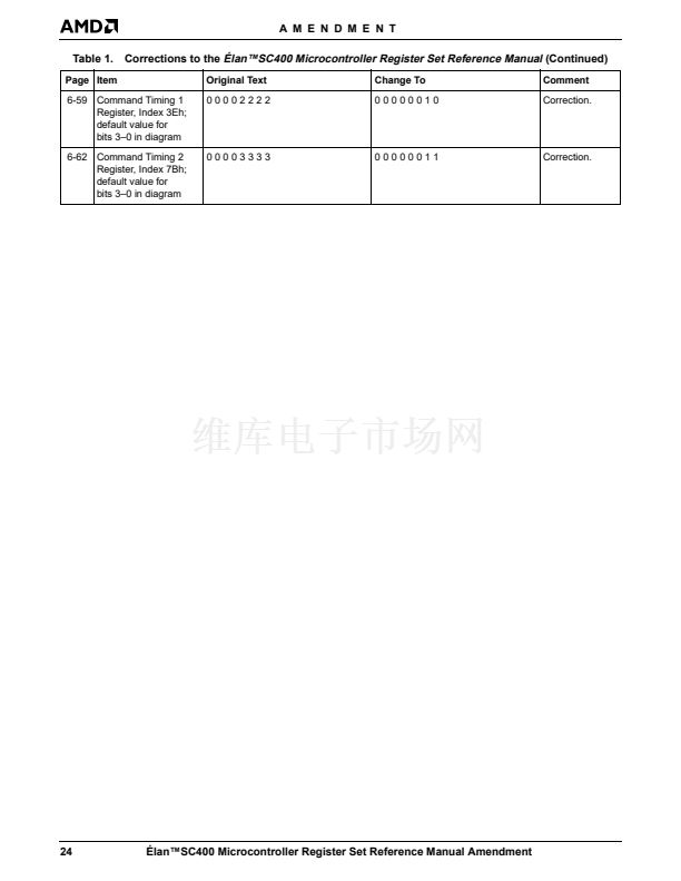
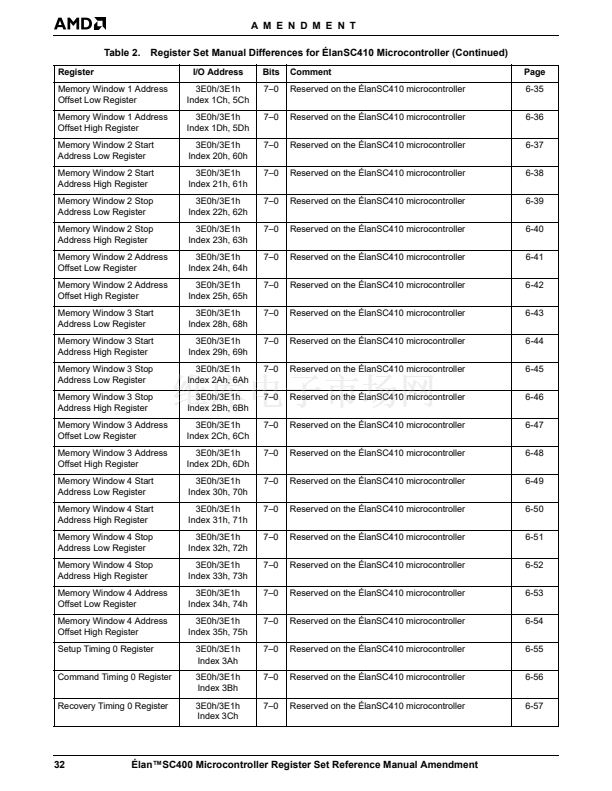
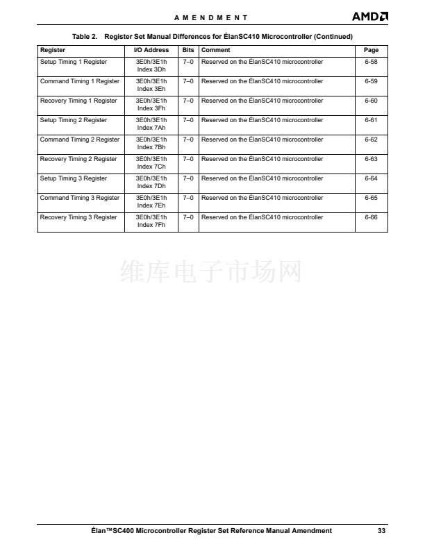
Table 1. Corrections to the
脡lan鈩C400 Microcontroller Register Set Reference Manual
Page Item
Title Page
Original Text
Change To
Comment
Add 脡lanSC410
microcontroller
to book title.
脡lan鈩C400 Microcontroller
Register Set Reference Manual
脡lan鈩C400 and 脡lanSC410
Microcontrollers Register Set
Reference Manual
Chapter 2: PC/AT-Compatible Direct-Mapped Registers
2-36 Programmable Interval
Timer #1 Channel 0
Count Register, Address
0040h; last paragraph
2-37 Programmable Interval
Timer #1 Channel 1
Count Register, Address
0041h; last paragraph
2-38 Programmable Interval
Timer #1 Channel 2
Count Register, Address
0042h; last paragraph
When set up for either BCD or 16-bit
binary count operation, the
maximum count for Channel 0 is
achieved by writing the internal
counting element associated with
this register to 0000h/d. See direct-
mapped register 43h for more detail.
When set up for either BCD or 16-bit
binary count operation, the
maximum count for Channel 0 is
achieved by writing the internal
counting element associated with
this register to 0. See direct-mapped
register 43h for more detail.
Same change
for all three
pages. Notation
鈥?000h/d鈥?is
misleading. Zero
value written
can be binary
(hex) or BCD
(decimal).
This document contains information on a product under development at Advanced Micro Devices. The information
is intended to help you evaluate this product. AMD reserves the right to change or discontinue work on this product
without notice.
Publication#
21032
Rev:
A
Amendment/1
Issue Date:
December 1997


 1
1
 2
2
 3
3
 4
4
 5
5
 6
6
 7
7
 8
8
 9
9
 10
10
 11
11
 12
12
 13
13
 14
14
 15
15
 16
16
 17
17
 18
18
 19
19
 20
20
 21
21
 22
22
 23
23
 24
24
 25
25
 26
26
 27
27
 28
28
 29
29
 30
30
 31
31
 32
32
 33
33
 34
34
 35
35
 36
36
 37
37
 38
38
 39
39
 40
40
