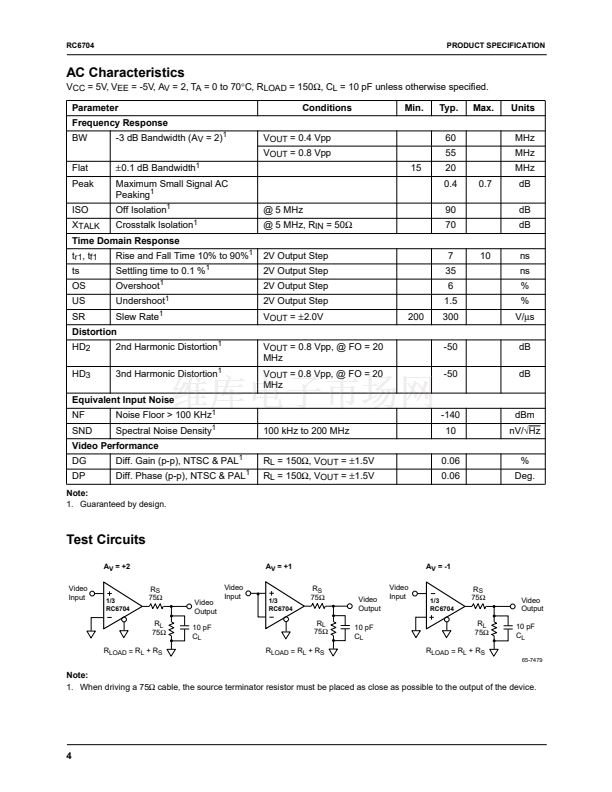
鈩?/div>
)
鈥?High CMRR (75 dB), High PSRR (70 dB)
鈥?Dual
鹵
5V power supply
鈥?Low offset 2.0 mV
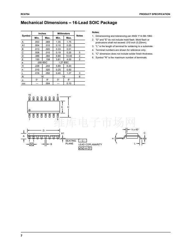
鈥?16-pin narrow SOIC package
鈥?300 V/
碌
s slew rate
鈥?Fast settling time: 0.1% in 35 ns
鈥?Voltage gain accuracy better than 0.5%
鈥?TTL or CMOS compatible enable inputs
Description
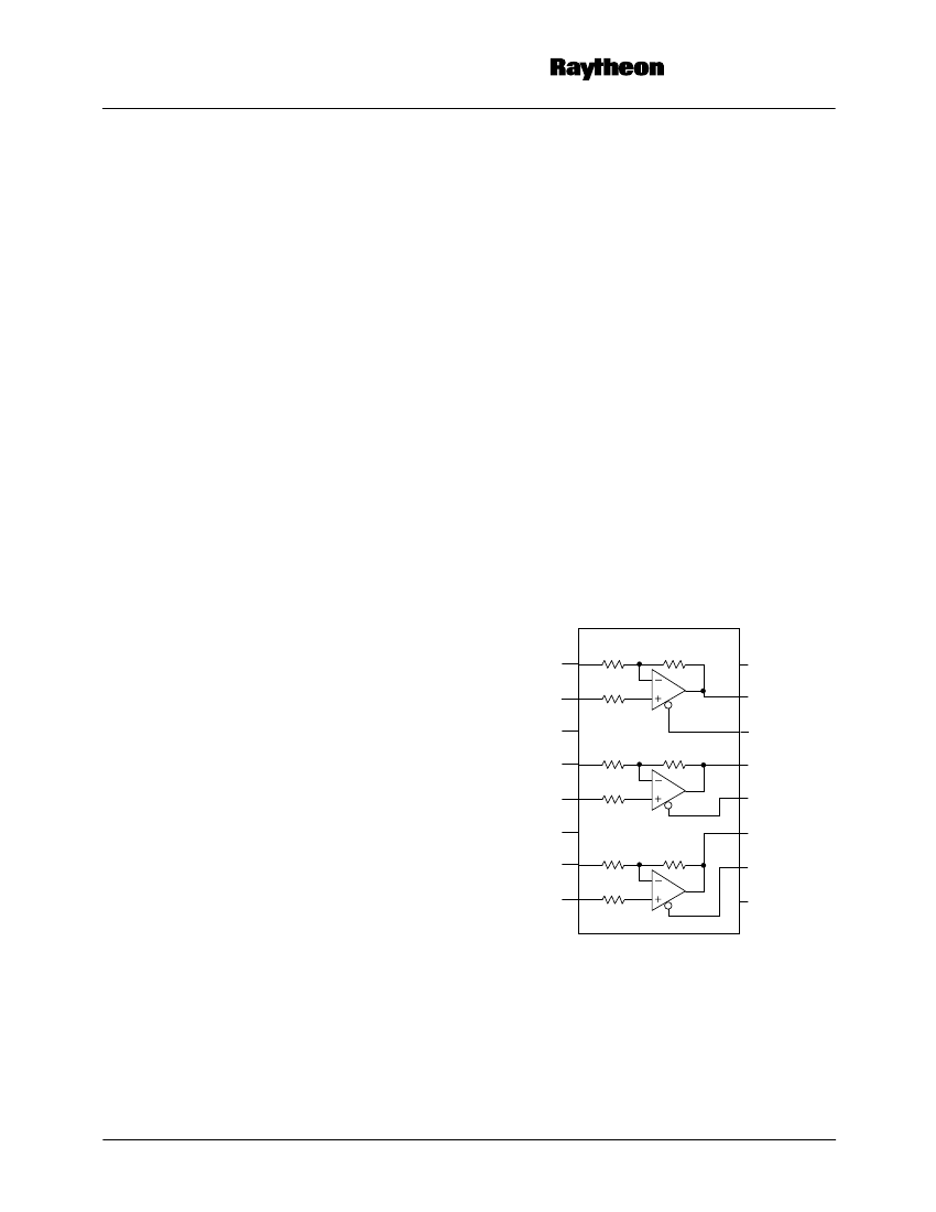
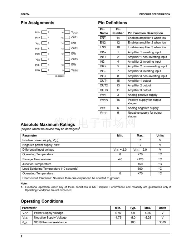
The RC6704 consists of three low power, wide band voltage
feedback operational ampli鏗乪rs. Internal thin-鏗乴m gain set-
ting resistors provide gains of +2, +1 and -1. Each channel is
capable of delivering a load current of at least 35mA.
Each ampli鏗乪r can be independently enabled or disabled
with a TTL or CMOS signal. When disabled, the ampli鏗乪r is
in a high impedance output state, presenting a very high
input to output isolation. The layout is optimized for low
channel to channel crosstalk.
The ampli鏗乪rs are optimized for video applications where
low differential gain and low phase distortion are signi鏗乧ant
requirements.
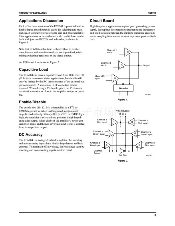
Applications
鈥?/div>
鈥?/div>
鈥?/div>
鈥?/div>
鈥?/div>
鈥?/div>
鈥?/div>
RGB ampli鏗乪r
3:1 crosspoint switch
RGB switch
Video instrumentation ampli鏗乪r
Selectable gain ampli鏗乪r
Programmable 鏗乴ter
Active 鏗乴ter
Block Diagram
R
R/2
OUT1
EN1
R
R/2
R
OUT2
EN2
OUT3
R
IN3鈥?/div>
R/2
IN3+
V
EEO
R
EN3
R
V
CCO
IN1鈥?/div>
IN1+
V
CC
IN2鈥?/div>
IN2+
V
EE
R = 500鈩?/div>
65-7450
Rev. 1.0.1


 1
1
 2
2
 3
3
 4
4
 5
5
 6
6
 7
7
 8
8
