Wide Effective Area, High Sensitivity Multialkali Photocathode
185 nm to 900 nm, 28 mm (1-1/8 Inch) Diameter, 9-stage, Side-on Type
GNew
Electro-Optical Design Structure
GWide
Effective Area ................................... 10 mm
脳
24 mm
GHigh
Cathode Sensitivity (Luminous) ..... 300
碌A(chǔ)/lm
GHigh
Anode Sensitivity (Luminous) ......... 3000 A/lm
GBasing
Diagram is same as the R928
FEATURES
APPLICATIONS
GSpectroscopy
GBiomedical
GEnvironmental
Monitoring
SPECIFICATIONS
GENERAL
Parameter
Spectral Response
Wavelength of Maximum Response
Photocathode MateriaI
Minimum Effective Area
Window Material
Dynode Structure
Number of Stages
Direct Interelectrode Capacitances
Anode to Last Dynode
Anode to All Other Electrodes
Base
SuitabIe Socket
SuitabIe D-Type Socket Assembly
Weight
Operating Ambient Temperature
Storage Temperature
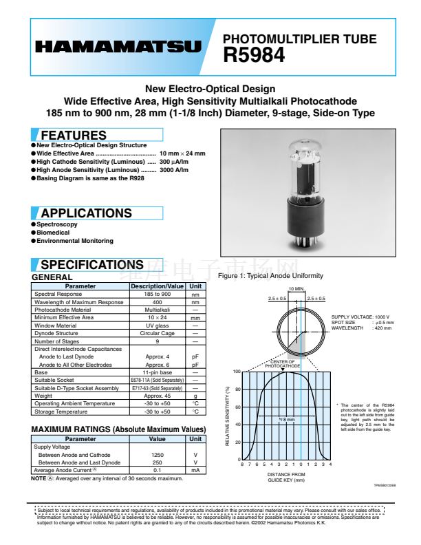
Figure 1: Typical Anode Uniformity
Description/Value Unit
185 to 900
400
Multialkali
10
脳
24
UV glass
Circular Cage
9
Approx. 4
Approx. 6
11-pin base
E678-11A (Sold Separately)
E717-63 (Sold Separately)
Approx. 45
-30 to +50
-30 to +50
nm
nm
鈥?/div>
mm
鈥?/div>
鈥?/div>
鈥?/div>
pF
pF
鈥?/div>
鈥?/div>
鈥?/div>
g
擄C
擄C
2.5
鹵
0.5
10 MIN.
2.5
鹵
0.5
SUPPLY VOLTAGE : 1000 V
SPOT SIZE
: 0.5 mm
WAVELENGTH
: 420 mm
CENTER OF
PHOTOCATHODE
100
RELATIVE SENSITIVITY (%)
80
60
8 mm
40
MAXIMUM RATINGS (Absolute Maximum Values)
Parameter
Value
Unit
V
V
mA
Supply Voltage
Between Anode and Cathode
1250
Between Anode and Last Dynode
250
A
Average Anode Current
0.1
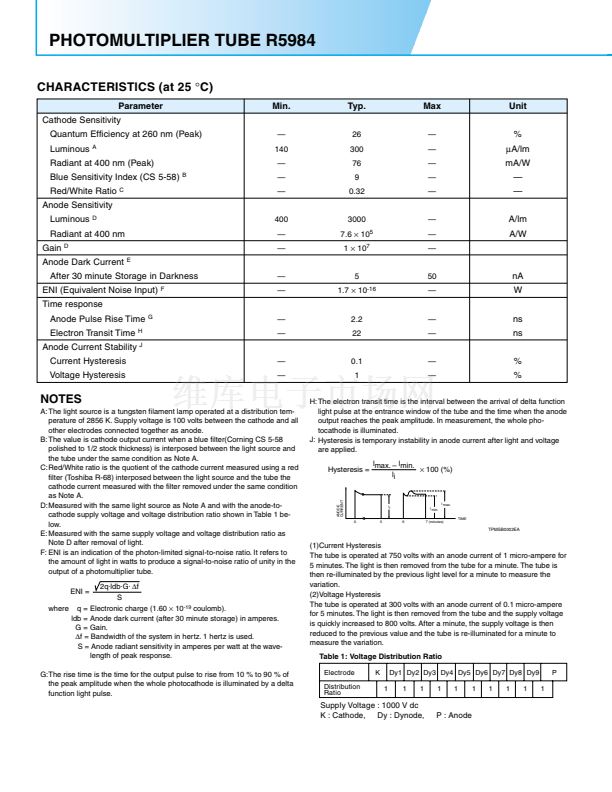
NOTE
A:
Averaged over any interval of 30 seconds maximum.
* The center of the R5984
photocathode is slightly laid
out to the left side from guide
key, light path should be
adjusted by 2.5 mm to the
left side from the guide key.
20
0
8
7
6
5
4
3
2
1
0
1
2
3
4
DISTANCE FROM
GUIDE KEY (mm)
TPMSB0122EB
Subject to local technical requirements and regulations, availability of products included in this promotional material may vary. Please consult with our sales office.
Information furnished by HAMAMATSU is believed to be reliable. However, no responsibility is assumed for possible inaccuracies or omissions. Specifications are
subject to change without notice. No patent rights are granted to any of the circuits described herein. 漏2002 Hamamatsu Photonics K.K.


 1
1
 2
2
 3
3
 4
4
