鈩?/div>
Pin compatibility with QS3245
250ps propagation delay
Undershoot clamp diodes on all switch and control inputs
LVTTL-compatible control inputs
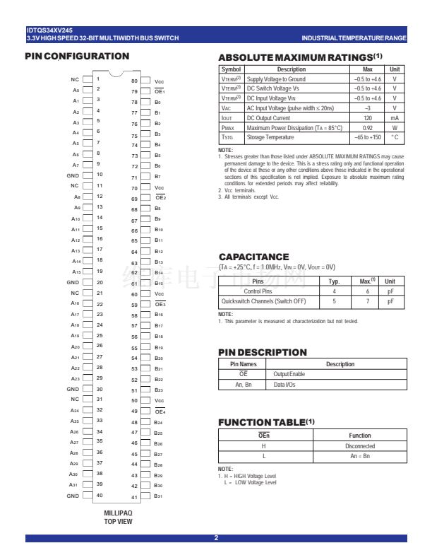
Available in 80-pin QVSOP package
DESCRIPTION:
APPLICATIONS:
鈥?3.3V to 2.5V Voltage translation
鈥?2.5V to 1.8V Voltage translation
鈥?PCI bus isolation hot swap
The QS34XV245 is a set of 32-bit high speed bus switches controlled by
LVTTL-compatible active low enable signal. When closed, the switches exhibit
near zero propagation delay without generating additional ground bounce or
switching noise.
The QS34XV245 is specially designed for direct interface betweeen 3.3V and
2.5V devices without any external components. When operating from a 3.3V
supply, the logic high level at the switch output is clamped to 2.5V when the switch
input signal exceeds 2.5V. This device can be used for switching 2.5V buses
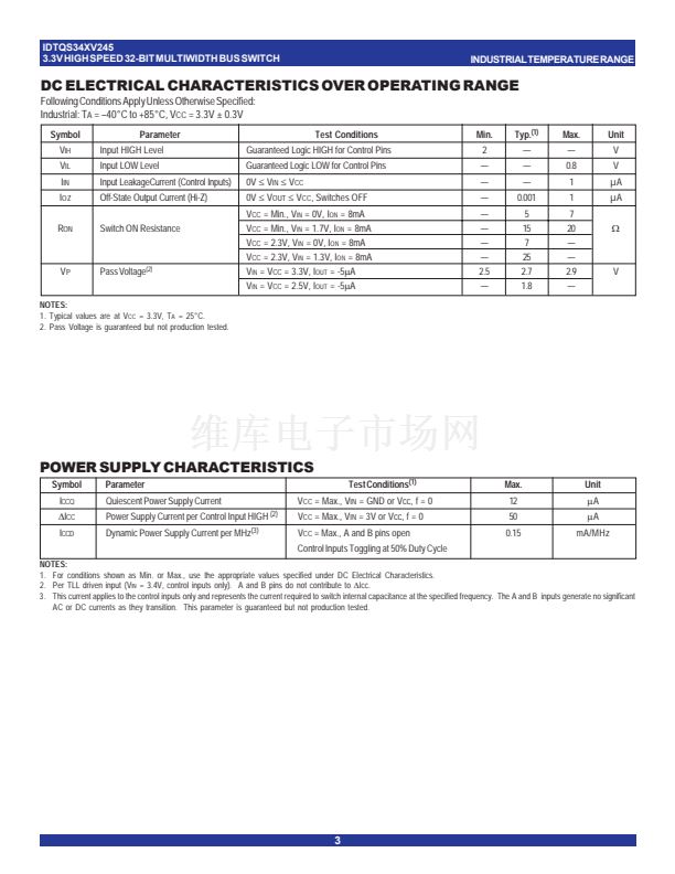
without signal attenuation. The ON resistance at 3.3V V
CC
is less than 5鈩?typical,
providing near zero propagation delay through the switch. Absence of DC path
from switch I/O pins to V
CC
or ground makes QS34XV245 an ideal device for
hot swapping applications.
The QS34XV245 is characterized for operation from -40擄C to +85擄C.
FUNCTIONAL BLOCK DIAGRAM
A0
A1
A2
A3
A4
A5
A6
A7
A 16
A 17
A 18
A 19
A 20
A 21 A 22
A 23
OE 1
OE 3
B0
B1
B2
B3
B4
B5
B6
B7
B 16
B 17
B 18
B 19
B 20
B 21 B 22
B 23
A8
A9
A 10 A 11
A 12
A 13 A 14 A 15
A 24
A 25
A 26
A 27
A 28
A 29 A 30
A 31
OE 2
OE 4
B8
B9
B 10 B 11
B 12
B 13 B 14 B 15
B24
B25
B 26
B 27
B 28
B 29 B 30
B 31
The IDT logo is a registered trademark of Integrated Device Technology, Inc.
INDUSTRIAL TEMPERATURE RANGE
1
c
1999 Integrated Device Technology, Inc.
NOVEMBER 1999
DSC-5580/1


 1
1
 2
2
 3
3
 4
4
 5
5
 6
6
 7
7
