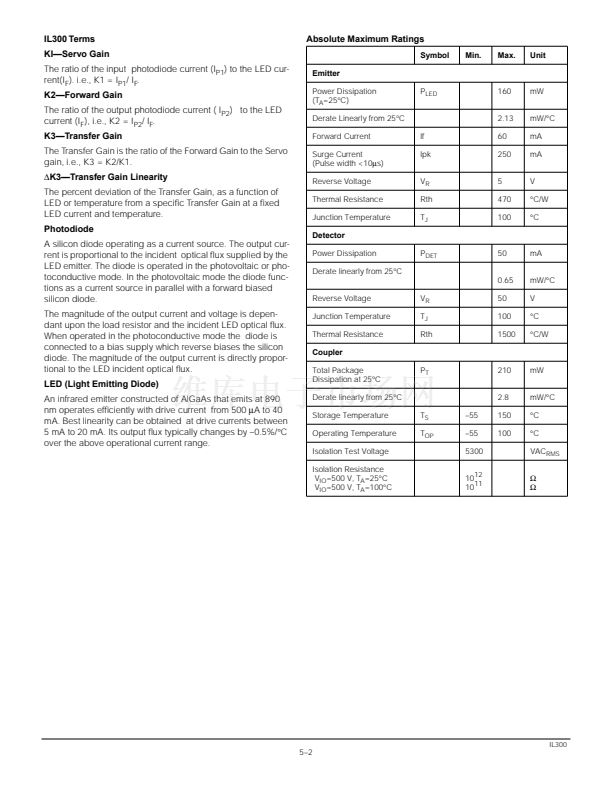
IL300
LINEAR OPTOCOUPLER
FEATURES
鈥?Couples AC and DC signals
鈥?0.01% Servo Linearity
鈥?Wide Bandwidth, >200 KHz
鈥?High Gain Stability,
鹵
0.005%/C
鈥?Low Input-Output Capacitance
鈥?Low Power Consumption, < 15mw
鈥?Isolation Test Voltage, 5300 VAC
RMS
,
1 sec.
鈥?Internal Insulation Distance, >0.4
mm
for VDE
鈥?Underwriters Lab File #E52744
鈥?VDE Approval #0884 (Optional with
Option 1, Add -X001 Suf鏗亁)
鈥?IL300G Replaced by IL300-X006
APPLICATIONS
鈥?Power Supply Feedback Voltage/
Current
鈥?Medical Sensor Isolation
鈥?Audio Signal Interfacing
鈥?Isolate Process Control Transducers
鈥?Digital Telephone Isolation
DESCRIPTION
The IL300 Linear Optocoupler consists of
an AlGaAs IRLED irradiating an isolated
feedback and an output PIN photodiode
in a bifurcated arrangement. The feed-
back photodiode captures a percentage
of the LED's 鏗倁x and generates a control
signal (IP
1
) that can be used to servo the
LED drive current. This technique com-
pensates for the LED's non-linear, time,
and temperature characteristics. The out-
put PIN photodiode produces an output
signal (IP
2
) that is linearly related to the
servo optical 鏗倁x created by the LED.
The time and temperature stability of the
input-output coupler gain (K3) is insured
by using matched PIN photodiodes that
accurately track the output 鏗倁x of the
LED.
A typical application circuit (Figure 1)
uses an operational ampli鏗乪r at the circuit
input to drive the LED. The feedback
photodiode sources current to R1 con-
nected to the inverting input of U1. The
photocurrent, IP1, will be of a magnitude
to satisfy the relationship of (IP1=V
IN
/R1).
Dimensions in inches (mm)
4
3
2
1
Pin One I.D.
1
8
.268 (6.81)
.255 (6.48)
5
6
7
8
2
3
4
.390 (9.91)
.379 (9.63)
.045 (1.14) .150 (3.81)
.030 (.76) .130 (3.30)
K1
K2
7
6
5
.305 Typ.
(7.75) Typ.
.135 (3.43)
.115 (2.92)
4擄 Typ.
.022 (.56)
.018 (.46)
.040 (1.02)
.030 (.76 )
.100 (2.54) Typ.
10擄 Typ.
3擄鈥?擄
.012 (.30)
.008 (.20)
DESCRIPTION
(continued)
The magnitude of this current is directly proportional to the feedback transfer gain
(K1) times the LED drive current (V
IN
/R1=K1 鈥?I
F
). The op-amp will supply LED cur-
rent to force suf鏗乧ient photocurrent to keep the node voltage (Vb) equal to Va
The output photodiode is connected to a non-inverting voltage follower ampli鏗乪r. The
photodiode load resistor, R2, performs the current to voltage conversion. The output
ampli鏗乪r voltage is the product of the output forward gain (K2) times the LED current
and photodiode load, R2 (V
O
=I
F
鈥?K2 鈥?R2).
Therefore, the overall transfer gain (V
O
/V
IN
) becomes the ratio of the product of the
output forward gain (K2) times the photodiode load resistor (R2) to the product of the
feedback transfer gain (K1) times the input resistor (R1). This reduces to V
O
/V
IN
=
(K2 鈥?R2)/(K1 鈥?R1). The overall transfer gain is completely independent of the LED
forward current. The IL300 transfer gain (K3) is expressed as the ratio of the ouput
gain (K2) to the feedback gain (K1). This shows that the circuit gain becomes the
product of the IL300 transfer gain times the ratio of the output to input resistors [V
O
/
V
IN
=K3 (R2/R1)].
Figure 1. Typical application circuit
Va
+
Vin
Vb
1
+
U1
V
CC
2
IF
V
CC
K1
3
4
lp 1
IL300
8
7
6
5
lp 2
V
CC
Vc
R2
K2
-
-
U2
+
V
CC
Vout
R1
5鈥?


 1
1
 2
2
 3
3
 4
4
 5
5
 6
6
 7
7
 8
8
