128 K x 32 Flash Module
PUMA68FV4006X - 70/90/12
Issue 5.0 January 2000
Description
The PUMA68 range of devices provide a high density
surface mount industry standard memory solution
which may accommodate various memory
technologies including SRAM, EEPROM and Flash.
The devices are designed to offer a defined upgrade
path and may be user configured as 8, 16 or 32 bits
wide.
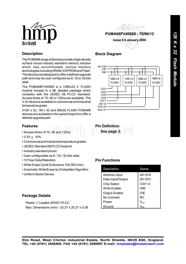
The PUMA68FV4006X is a 128Kx32 3. FLASH
module housed in a 68 Jleaded package which
complies with the JEDEC 68 PLCC standard.
Access times of 70, 90 or 120ns are available. The
3.3V device is available to commercial and industrial
temperature grade.
512K x 32, 1M x 32 and 2Mx32 FLASH PUMA68
devices are available in the same footprint to offer a
defined upgrade path.
Block Diagram
A0~A16
/OE
/WE
128K x 8
FLASH
/CS1
/CS2
/CS3
/CS4
D0~7
D8~15
D16~23
D24~31
128K x 8
FLASH
128K x 8
FLASH
128K x 8
FLASH
Features
鈥?Access times of 70, 90 and 120ns.
鈥?3.3V + 10%.
鈥?Commercial and Industrial temperature grades
鈥?JEDEC Standard 68 PLCC footprint.
鈥?Industry standard pinout.
鈥?User configurable as 8 / 16 / 32 bits wide.
鈥?10 Year Data Retention
鈥?Write Erase Cycle Endurance 100,000 (min)
鈥?Automatic Write/Erase by Embedded Algorithm
鈥?Uniform Sector Device.
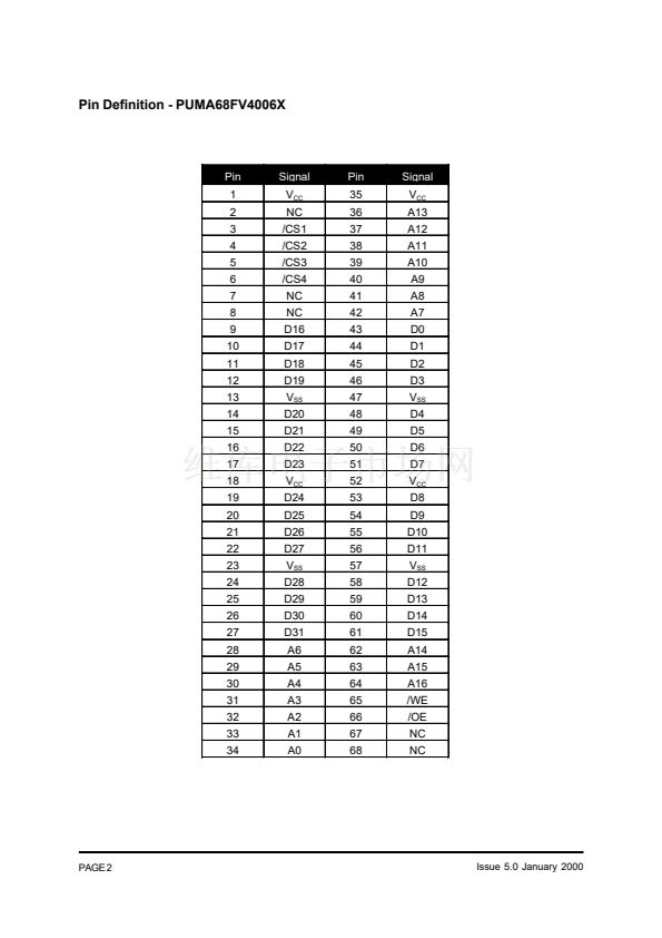
Pin Definition
See page 2.
Pin Functions
Description
Address Input
Data Input/Output
Chip Select
Write Enable
Output Enable
No Connect
Power
Ground
Signal
A0~A16
D0~D31
/CS1~4
/WE
/OE
NC
V
CC
V
SS
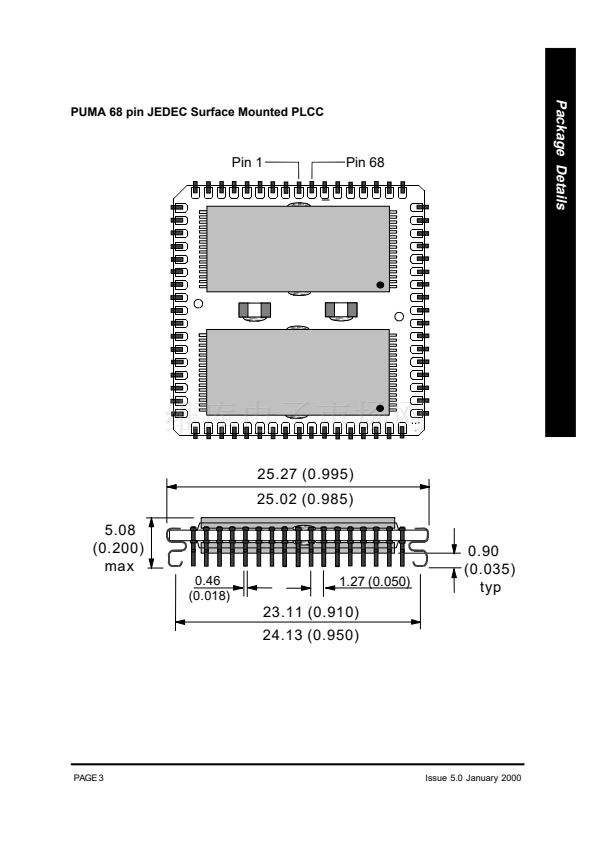
Package Details
Plastic 鈥楯鈥?Leaded JEDEC PLCC
Max. Dimensions (mm) - 25.27 x 25.27 x 5.08
Elm Road, West Chirton Industrial Estate, North Shields, NE29 8SE, England.
TEL +44 (0191) 2930500. FAX +44 (0191) 2590997 E-mail:
hmpsales@mosaicsemi.com


 1
1
 2
2
 3
3
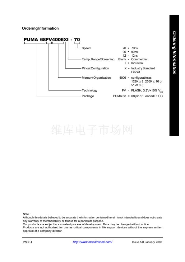 4
4
 5
5
