128K x 32 FLASH Memory
PUMA 2F4006-70/90/12
Elm Road, West Chirton, NORTH SHIELDS, Tyne & Wear
NE29 8SE, England Tel. +44 (0)191 2930500 Fax. +44 (0) 191 2590997
Issue 4.1 April 1999
General Description
The PUMA 2F4006 is a 4,194,304 bit CMOS 5.0V
only FLASH memory in a 66 pin ceramic PGA
package, which is configurable as 8, 16, 32 bit wide
output using four chip selects.Flash memory
combines the functionality of EEPROM with on chip
electrical Write/Erase logic, thus simplifying the
external control circuitry. The PUMA 2F4006
incorporates Automatic Programming and Erase
functions, which allow up to 10,000 Write/Erase
cycles (min).
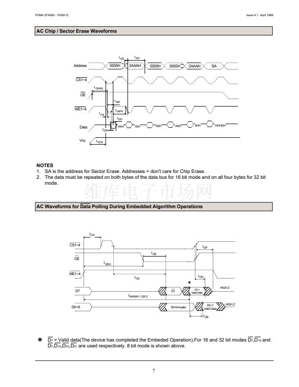
In addition, a Sector Erase function is available
which can erase one 16K block of data randomly
and more than one block simultaneously. The PUMA
2F4006 also features hardware sector protection,
which enables both program and erase operations in
any of the 32 sectors on the module.
Features
鈥?Very Fast Access Times of 70ns/90ns/120ns.
鈥?Operating Power (Read) 660 mW (Max)
(Program/Erase) 1100 mW (Max)
Standby Power
2.2 mW (Max)
Output Configurable as 32 / 16 / 8 bit wide.
鈥?Automatic Write/Erase by Embedded Algorithm -
end of Write/Erase indicated by DATA Polling and
Toggle Bit.
鈥?Flexible Sector Erase Architecture - 16K byte sector
size, with hardware protection of any number of
sectors.
鈥?Single Byte Program of 14碌s (typical), Sector Pro
gram time of 0.3 sec. (typical).
鈥?Module FLASH Erase of 3 seconds (typical).
鈥?Erase/Write Cycle Endurance 10,000 (minimum)
鈥?Can be screened in accordance with MIL-STD-883.
Block Diagram
Pin Definition
A0~A16
OE
WE4
WE3
WE2
WE1
1
12
23
34
45
56
D8
2
WE2
13
D15
24
D24
35
VCC
46
D31
57
D9
3
CS2
14
D14
25
D25
36
CS4
47
D30
58
D10
4
GND
15
D13
26
D26
37
WE4
48
D29
59
A14
D11
16
D12
27
A7
D27
49
D28
60
128K x 8
FLASH
CS1
CS2
CS3
CS4
D0~7
D8~15
D16~23
D24~31
128K x 8
FLASH
128K x 8
FLASH
128K x 8
FLASH
5
A16
6
A10
17
OE
28
A11
7
A9
18
NC
29
VIEW
FROM
ABOVE
38
A12
39
A4
50
A1
61
NC
40
A5
51
A2
62
A0
8
A15
19
WE1
30
A13
41
A6
52
A3
63
NC
9
VCC
20
D7
31
A8
42
WE3
53
D23
64
D0
10
CS1
21
D6
32
D16
43
CS3
54
D22
65
D1
11
NC
22
D5
33
D17
44
GND
55
D21
66
D2
D3
D4
D18
D19
D20
Pin Functions
A0~A16
CS1~4
WE1~4
GND
Address Inputs
Chip Select
Write Enable
Ground
D0~D31
OE
V
CC
Data Input/Output
Output Enable
Power (+5V)


 1
1
 2
2
 3
3
 4
4
 5
5
 6
6
 7
7
 8
8
 9
9
 10
10
 11
11
 12
12
 13
13
 14
14
 15
15
 16
16
 17
17
 18
18
 19
19
 20
20
 21
21
 22
22
 23
23
 24
24
