錚?/div>
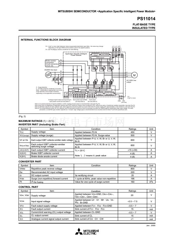
INTEGRATED DRIVE, PROTECTION AND SYSTEM CONTROL FUNCTIONS:
鈥?For inverter side upper-leg IGBTs : Drive circuit, High voltage isolated high-speed level shifting, Short circuit protection (SC).
Bootstrap circuit supply scheme (single drive power supply) and Under voltage protection (UV).
鈥?For inverter side lower-leg IGBTs : Drive circuit, Short circuit protection (SC).
Control supply circuit under- & over- voltage protection (OV/UV).
System over temperature protection (OT). Fault output signaling circuit (F
O
) and Current limit warn-
ing signal output (CL).
鈥?For Brake circuit IGBT : Drive circuit
鈥?Warning and Fault signaling :
F
O1
: Short circuit protection for lower-leg IGBTs and Input interlocking against spurious arm shoot-through.
F
O2
: N-side control supply abnormality locking (OV/UV).
F
O3
: System over-temperature protection (OT).
CL : Warning for inverter current overload condition
鈥?For system feedback control : Analogue signal feedback reproducing actual inverter output phase currents (3蠁).
鈥?Input Interface : 5V CMOS/TTL compatible, Schmitt trigger input, and Arm-Shoot-Through interlock protection.
APPLICATION
Acoustic noise-less 0.75kW/AC200V class 3 phase inverter and other motor control appli-
cations
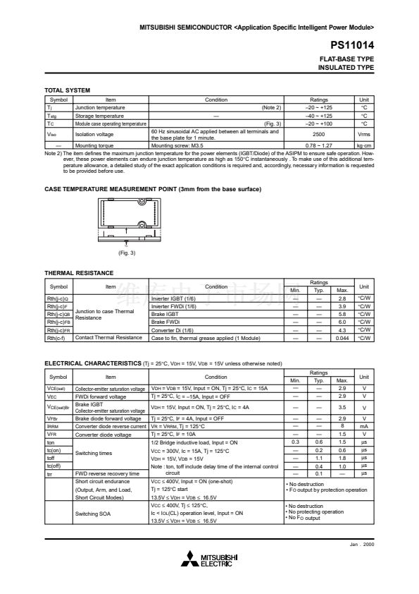
PACKAGE OUTLINES
4-R2
0.5
V
6
56
7 8 91011121314151617181920212223
Terminals Assignment:
1
2
3
4
5
6
7
8
9
10
11
12
13
14
15
16
17
18
19
20
CBU+
CBU鈥?/div>
CBV+
CBV鈥?/div>
CBW+
CBW鈥?/div>
GND
NC
VDH
CL
FO1
FO2
FO3
CU
CV
CW
UP
VP
WP
UN
21 VN
22 WN
23 Br
12 3 4
2424
24
5
94.2
鹵
1
82
鹵
0.8
50
V
0.5
2
鹵
0.3
2-蠁4
2-R4
5.08
鹵
0.3
!
9 = 45.72
鹵
0.8
31
32 33 34 35 36 37 38 39 40
1.2
V
Control Pin top
portion details
0~0.8
(16.25)
31
32
33
34
35
36
37
38
39
40
R
S
T
P1
P2
N
B
U
V
W
V
0.6
29
22.6
5
8.5
20.4
鹵
1
12
27
鹵
1
V
Main terminal top
portion details
0.8
鹵
0.5
0
3.5
LABEL
54
鹵
0.5
62
鹵
1
0.3
0~0.8
0.35MAX
0.4
12
鹵
0.5
0
0.5
0.6
0.5
鹵
0.03
(Fig. 1)
Jan . 2000


 1
1
 2
2
 3
3
 4
4
 5
5
 6
6
