Phototransistors
PNZ0155
Silicon NPN Phototransistor
Unit : mm
Not soldered 0.8 max.
For optical control systems
1.5鹵0.2
2.1鹵0.15
1.6鹵0.15
0.8鹵0.1
Features
High sensitivity
Wide spectral sensitivity, suited for detecting GaAs LEDs
Low dark current
12.8 min.
3.9鹵0.25
4.5鹵0.15
3.5鹵0.15
Flat type plastic package
(2.95)
2-1.2鹵0.3
2-0.45鹵0.15
1
2
2.54鹵0.2
0.45鹵0.2
Absolute Maximum Ratings
(Ta = 25藲C)
Parameter
Collector to emitter voltage
Emitter to collector voltage
Collector current
Collector power dissipation
Operating ambient temperature
Storage temperature
Symbol
V
CEO
V
ECO
I
C
P
C
T
opr
T
stg
Ratings
20
5
10
100
鈥?5 to +85
鈥?0 to +100
Unit
V
V
mA
mW
藲C
藲C
1: Emitter
2: Collector
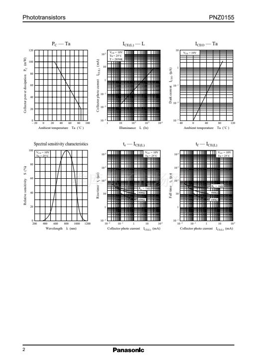
Electro-Optical Characteristics
(Ta = 25藲C)
Parameter
Dark current
Collector photo current
Peak sensitivity wavelength
Acceptance half angle
Response time
Collector saturation voltage
*1
*2
Symbol
I
CEO
I
CE(L)*1
位
P
胃
t
r
, t
f
*2
Conditions
V
CE
= 10V
V
CE
= 10V, L = 100 lx
V
CE
= 10V
Measured from the optical axis to the half power point
V
CC
= 10V, I
CE(L)
= 1mA, R
L
= 100鈩?/div>
I
CE(L)
= 1mA, L = 1000 lx
min
0.05
typ
0.01
0.2
800
70
4
0.2
max
1
Unit
碌A(chǔ)
mA
nm
deg.
碌s
V
CE(sat)*1
0.5
V
Measurements were made using a tungsten lamp (color temperature T = 2856K) as a light source.
Switching time measurement circuit
Sig.IN
V
CC
(Input pulse)
Sig.OUT (Output pulse)
90%
10%
t
d
t
r
t
f
t
d
: Delay time
t
r
: Rise time (Time required for the collector photo current to
increase from 10% to 90% of its final value)
t
f
: Fall time (Time required for the collector photo current to
decrease from 90% to 10% of its initial value)
,,
,,
,,
next


 1
1
 2
2
