Phototransistors
PNA1801
Silicon NPN Phototransistor
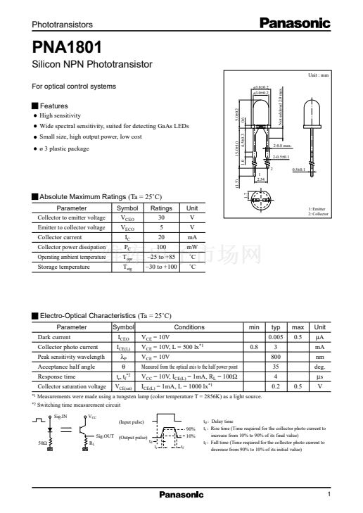
Unit : mm
Not soldered 2.0 max.
For optical control systems
Features
High sensitivity
Wide spectral sensitivity, suited for detecting GaAs LEDs
Small size, high output power, low cost
酶 3 plastic package
15.0鹵1.0
4.5鹵0.3
酶3.8鹵0.2
酶3.0鹵0.2
5.0鹵0.2
0.6
2-0.8 max.
2-0.5鹵0.1
2
0.5鹵0.1
1.0
(1.5)
1
2.54
Absolute Maximum Ratings
(Ta = 25藲C)
Parameter
Collector to emitter voltage
Emitter to collector voltage
Collector current
Collector power dissipation
Operating ambient temperature
Storage temperature
Symbol
V
CEO
V
ECO
I
C
P
C
T
opr
T
stg
Ratings
30
5
20
100
鈥?5 to +85
鈥?0 to +100
Unit
V
V
mA
mW
藲C
藲C
1.7
1: Emitter
2: Collector
Electro-Optical Characteristics
(Ta = 25藲C)
Parameter
Dark current
Collector photo current
Peak sensitivity wavelength
Acceptance half angle
Response time
Collector saturation voltage
*1
*2
Symbol
I
CEO
I
CE(L)
位
P
胃
t
r
, t
f*2
V
CE(sat)
V
CE
= 10V
Conditions
V
CE
= 10V, L = 500 lx
*1
V
CE
= 10V
Measured from the optical axis to the half power point
V
CC
= 10V, I
CE(L)
= 1mA, R
L
= 100鈩?/div>
I
CE(L)
= 1mA, L = 1000 lx
*1
min
0.8
typ
0.005
3
800
35
4
0.2
max
0.5
Unit
碌A(chǔ)
mA
nm
deg.
碌s
0.5
V
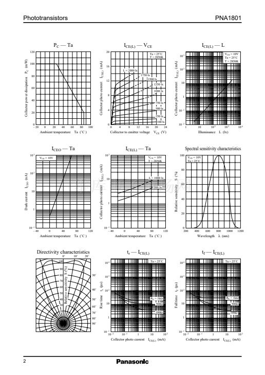
Measurements were made using a tungsten lamp (color temperature T = 2856K) as a light source.
Switching time measurement circuit
Sig.IN
V
CC
(Input pulse)
Sig.OUT (Output pulse)
90%
10%
t
d
t
r
t
f
t
d
: Delay time
t
r
: Rise time (Time required for the collector photo current to
increase from 10% to 90% of its final value)
t
f
: Fall time (Time required for the collector photo current to
decrease from 90% to 10% of its initial value)
,,
,,
,,
next


 1
1
 2
2
