frequency synthesizer. The PLL provide frequency
multiplication capabilities. The output clock frequency
鈥?/div>
0.13um CMOS device technology
鈥?1.2 Volt single power supply
鈥?Output frequency range: 20M ~ 100MHz
鈥?Jitter: 鹵200ps at 100MHz
鈥?Duty ratio: 40% to 60% (All tuned range)
FOUT=(m*FIN) / (p*2 )
Where FOUT is the output clock frequency. FIN is
the input clock frequency. m, p and s are the values
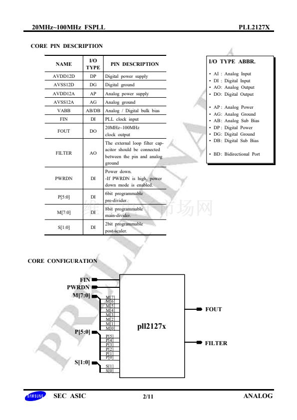
for programmable dividers. pll2127x consists of a
Phase Frequency Detector(PFD), a Charge Pump, an
Off-chip Loop Filter, a Voltage Controlled Oscillator
(VCO), a 6bit Pre-divider, an 8bit Main-divider and
2bit Post-scaler as shown in functional block diagram.
s
鈥?Power down mode
鈥?Off-chip loop filter
鈥?Frequency is changed by programmable divider
NOTE
1.
Don't set the P or M as zero, that is 000000 / 00000000
2. The proper range of P and M : 1<=P<=62, 1<=M<=248
3. The P and M must be selected considering stability of PLL and VCO output frequency range
4. Please consult with SEC application engineer to select the proper P, M and S values
No responsibility is assumed by SEC for its use nor for any infringements of patents or other rights of third parties that
may result from its use. The contents of the datasheet is subject to change without any notice.
FUNCTIONAL BLOCK DIAGRAM
AVDD12D
Fin/P
AVSS12D
UP
FILTER
R1
Charge
Pump
DN
FIN
Pre-Divider
(P)
Fvco/M
Phase
Frequency
Detector
C2
6b
M[7:0]
P[5:0]
S[1:0]
8b
PWRDN
Post - Scaler
(S)
(1,2,4,8)
AVDD12A
AVSS12A
VABB
2b
FOUT
Main-Divider
(M)
Fvco
Voltage
Controlled
Oscillator
Vctrl
SAMSUNG ELECTRONICS Co. LTD


 1
1
 2
2
 3
3
 4
4
 5
5
 6
6
 7
7
 8
8
 9
9
 10
10
 11
11
