USE ULTRA37000鈩?FOR
ALL NEW DESIGNS
PLDC20G10B
PLDC20G10
CMOS Generic 24-Pin Reprogrammable
Logic Device
Features
鈥?Fast
鈥?Commercial: t
PD
= 15 ns, t
CO
= 10 ns, t
S
= 12 ns
鈥?Military: t
PD
= 20 ns, t
CO
= 15 ns, t
S
= 15 ns
鈥?Low power
鈥?I
CC
max.: 70 mA, commercial
鈥?I
CC
max.: 100 mA, military
鈥?Commercial and military temperature range
鈥?User-programmable output cells
鈥?Selectable for registered or combinatorial operation
鈥?Output polarity control
鈥?Output enable source selectable from pin 13 or
product term
鈥?Generic architecture to replace standard logic
functions including: 20L10, 20L8, 20R8, 20R6, 20R4,
12L10, 14L8, 16L6, 18L4, 20L2, and 20V8
鈥?Eight product terms and one OE product term per output
鈥?CMOS EPROM technology for reprogrammability
鈥?Highly reliable
鈥?Uses proven EPROM technology
鈥?Fully AC and DC tested
鈥?Security feature prevents logic pattern duplication
鈥?/div>
鹵10%
power supply voltage and higher noise
immunity
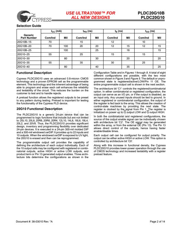
Functional Description
Cypress PLD devices are high-speed electrically program-
mable logic devices. These devices utilize the sum-of-products
(AND-OR) structure providing users the ability to program
custom logic functions for unique requirements.
In an unprogrammed state the AND gates are connected via
EPROM cells to both the true and complement of every input.
By selectively programming the EPROM cells, AND gates may
be connected to either the true or complement or disconnected
from both true and complement inputs.
I
6
I
5
I
4
I
3
I
2
CP/I
1
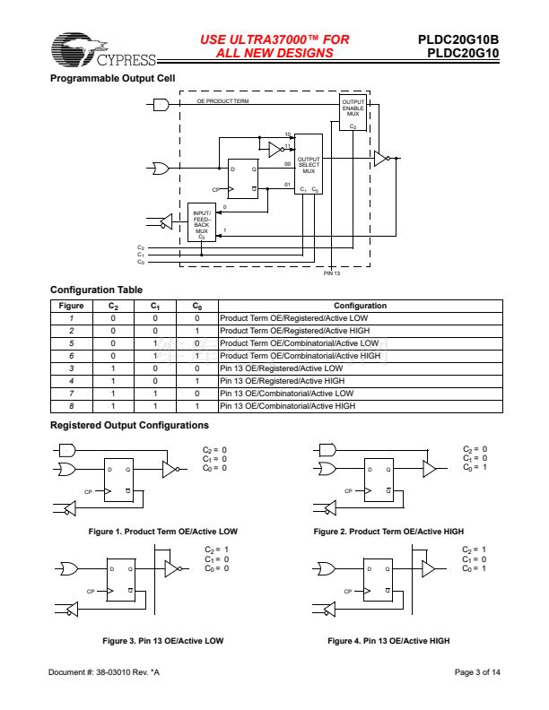
Logic Block Diagram
V
SS
12
I
11
I
10
I
9
I
8
I
7
PROGRAMMABLE
AND ARRAY
8
8
8
OE
OUTPUT
CELL
OUTPUT
CELL
8
OE
OUTPUT
CELL
8
OE
OUTPUT
CELL
8
OE
OUTPUT
CELL
8
OE
8
OE
8
OE
OUTPUT
CELL
8
OE
OUTPUT
CELL
OUTPUT
CELL
OUTPUT
CELL
OUTPUT
CELL
13
I/OE
14
I/O
9
15
I/O
8
16
I/O
7
17
I/O
6
18
I/O
5
19
I/O
4
20
I/O
3
21
I/O
2
22
I/O
1
23
I/O
0
24
V
CC
Pin Configurations
LCC
Top View
NC
I
I
CP/I
V
CC
I/O 0
I/O 1
STD PLCC
Top View
I
I
I
CP/I
V CC
I/O0
I/O1
JEDEC PLCC
Top View
I
I
CP/I
NC
V CC
I/O0
I/O 1
4 3 2 1 2827 26
I/O
2
I/O
3
I/O
4
I/O
5
I/O
6
I/O
7
NC
I
I
I
NC
I
I
I
5
6
7
8
9
10
11
[1]
I
I
I
I
I
I
NC
5
6
7
8
9
10
11
4 3 2 1 282726
25
24
23
PLDC20G10 22
PLDC20G10B
21
20
19
12131415161718
V SS
I/OE
I/O9
I/O8
NC
4 3 2 1 2827 26
NC
I/O
2
I/O
3
I/O
4
I/O
5
I/O
6
I/O
7
NC
I
I
NC
I
I
NC
5
6
7
8
9
10
11
25
24
23
PLDC20G10
PLDC20G10B 22
21
20
121314 1516 1718 19
V
SS
I/OE
I/O 9
I/O 8
I
I
I
25
24
23
CG7C323鈥揂
CG7C323B鈥揂 22
21
20
121314 1516 1718 19
VSS
NC
I/OE
I/O 9
I/O 8
I
I
I/O
2
I/O
3
I/O
4
NC
I/O
5
I/O
6
I/O
7
Note:
1. The CG7C323 is the PLDC20G10 packaged in the JEDEC-compatible 28-pin PLCC pinout. Pin function and pin order is identical for both PLCC pinouts. The
difference is in the location of the 鈥渘o connect鈥?or NC pins.
Cypress Semiconductor Corporation
Document #: 38-03010 Rev. *A
I
I
鈥?/div>
3901 North First Street
鈥?/div>
San Jose
,
CA 95134
鈥?/div>
408-943-2600
Revised April 20, 2004


 1
1
 2
2
 3
3
 4
4
 5
5
 6
6
 7
7
 8
8
 9
9
 10
10
 11
11
 12
12
 13
13
 14
14
