PJ494
Switchmode Pulse Width Modulation Control Circuit
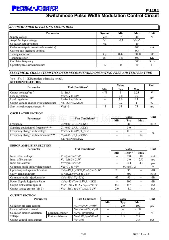
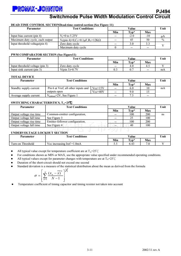
he PJ494 incorporates on a single monolithic chip all
the functions required in the construction of a pulse-
width-modulation control circuit. Designed primarily for
power supply control, these devices offer the systems
engineer the flexibility to tailor the power supply control
circuitry to his application.
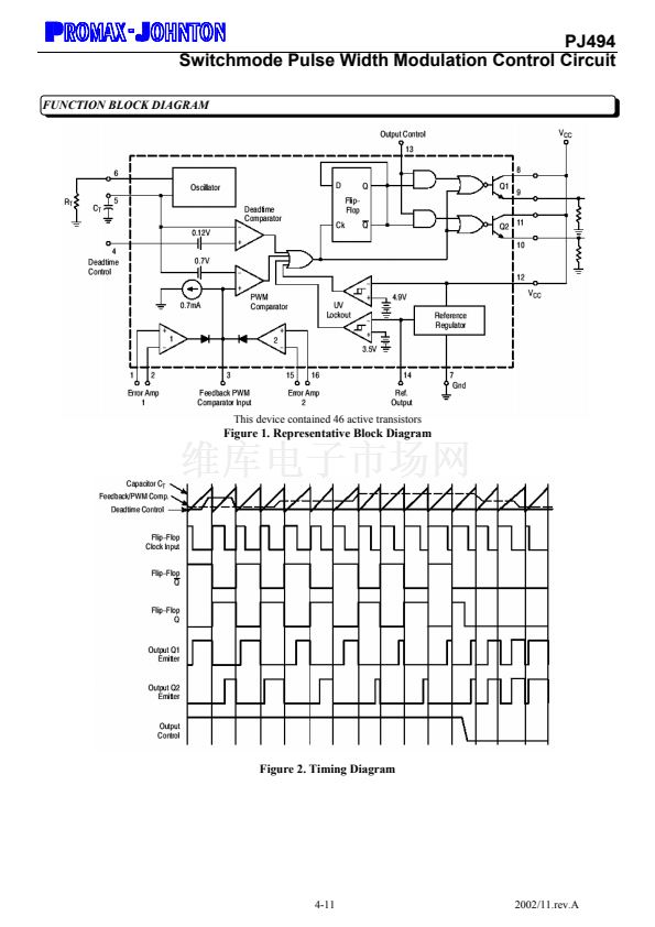
The PJ494 contains an error amplifier, an on-chip adjustable
oscillator, a deed-time control comparator, pulse-steering
control flip-flop, a 5-volt, 5% precision regulator, and output-
control circuits. The error amplifier exhibits a common-mode
voltage from 鈥?.3 volts to Vcc 鈥? volts. The dead-time
control comparator has a fixed offset that provides
T
approximately 5% dead time when externally altered. The on-
chip oscillatory be bypassed by terminating R
T
(pin 6) to the
reference output and providing a sawtooth input to C
T
(PIN
5), or it may be used to drive the common circuits in
synchronous multiple-rail power supplies. The uncommited
output transistor provide either common-emitter or emitter-
follower output capability. Each device provides for push-pull
or single-ended output operation, which may be selected
through the output-control function. The architecture of these
devices prohibits the possibility of either output being pulsed
twice during push-pull operation.
FEATURES
鈥?/div>
鈥?/div>
鈥?/div>
鈥?/div>
鈥?/div>
鈥?/div>
鈥?/div>
Complete PWM Power Control Circuitry
Uncommitted Outputs for 200mA Sink or Source Current
Output Control Selects Single-Ended or Push 鈥揚(yáng)ull Operation
Internal Circuitry Prohibits Double Pulse at Either Output
Variable Dead-Time Provides Control over Total Range
Internal Regulator Provides a Stable 5-V Reference Supply, 5%
Circuit Architecture Allows Easy Synchronization
OperatingTemperature
(Ambient)
PJ494CD
PJ494CS
-20鈩?to +85鈩?/div>
DIP-16
SOP-16
Package
DIP-16
SOP-16
ORDERING INFORMATION
Device
Pin 1.Noninv Input
2.Inv Input
3.Feedback
5.C
T
8.C1
11.C2
13.Output Control
15. Inv Input
16. Noninv Input
錒?/div>
Error Amp1
4.Dead-Time Control
6.R
T
7.Gnd
9.E1
10.E2
12.Vcc
14.Ref Out
錒?/div>
Error Amp2
ABSOLUTE MAXIMUM RATINGS OVER OPERATING FREE-AIR TEMPERATURE RANGE
(unless otherwise noted)
Rating
Supply voltage
Amplifier input voltage
Collector output voltage
Collector output current
Operating free-air temperature range
Storage temperature range
Operating Junction Temperature
Lead temperature 1,6mm from case for 10 seconds
Power Dissipation @T
A
鈮?5鈩?/div>
P
D
T
stg
T
J
Symbol
Vcc
Vi
Vo
Value
41
Vcc+0.3
41
250
-20 to 85
-25 to 125
125
260
1000
mW
鈩?/div>
mA
Unit
V
1-11
2002/11.rev.A
PJ494相關(guān)型號(hào)PDF文件下載


 1
1
 2
2
 3
3
 4
4
 5
5
 6
6
 7
7
 8
8
 9
9
 10
10
 11
11
