Philips Semiconductors
Product specification
Logic level TOPFET
PIP3106-D
DESCRIPTION
Monolithic temperature and
overload protected logic level power
MOSFET in
TOPFET2
technology
assembled in a 3 pin surface mount
plastic package.
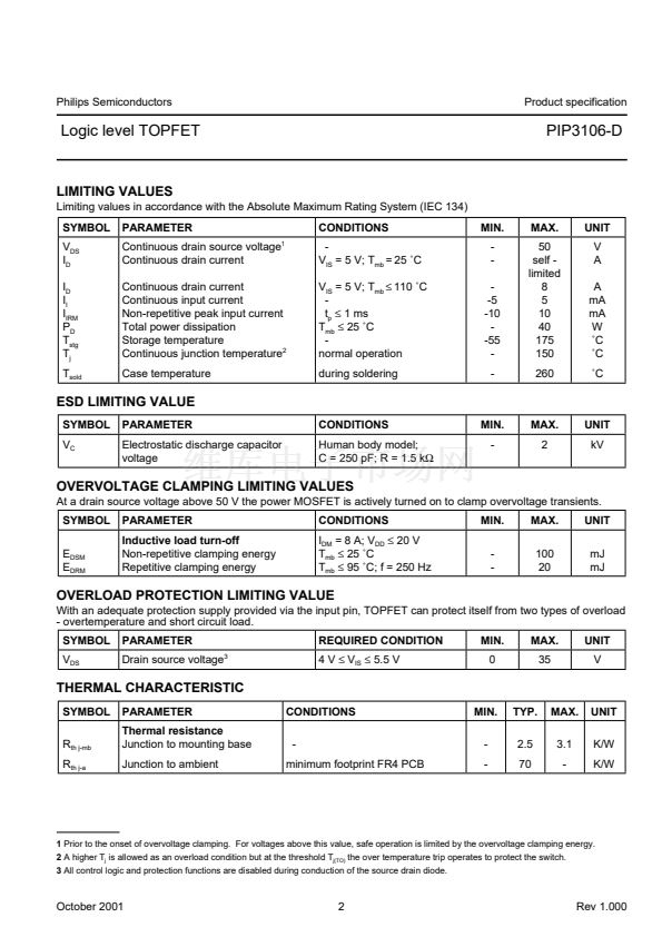
QUICK REFERENCE DATA
SYMBOL
V
DS
I
D
P
D
T
j
R
DS(ON)
I
ISL
PARAMETER
Continuous drain source voltage
Continuous drain current
Total power dissipation
Continuous junction temperature
Drain-source on-state resistance
Input supply current
V
IS
= 5 V
MAX.
50
8
40
150
100
650
UNIT
V
A
W
藲C
m鈩?/div>
碌A(chǔ)
APPLICATIONS
General purpose switch for driving
lamps
motors
solenoids
heaters
FEATURES
TrenchMOS output stage
Current limiting
Overload protection
Overtemperature protection
Protection latched reset by input
5 V logic compatible input level
Control of output stage and
supply of overload protection
circuits derived from input
Low operating input current
permits direct drive by
micro-controller
ESD protection on all pins
Overvoltage clamping for turn
off of inductive loads
FUNCTIONAL BLOCK DIAGRAM
DRAIN
O/V
CLAMP
INPUT
RIG
POWER
MOSFET
LOGIC AND
PROTECTION
SOURCE
Fig.1. Elements of the TOPFET.
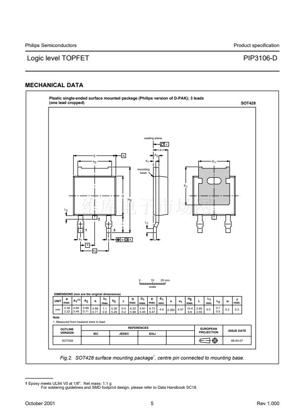
PINNING - SOT428
PIN
1
2
3
tab
input
drain
source
DESCRIPTION
PIN CONFIGURATION
tab
SYMBOL
D
TOPFET
I
P
2
drain
1
3
S
October 2001
1
Rev 1.000


 1
1
 2
2
 3
3
 4
4
 5
5
 6
6
