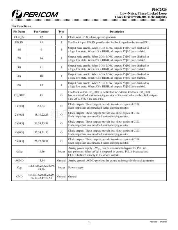
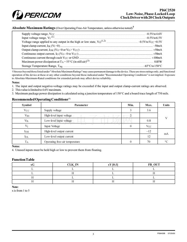
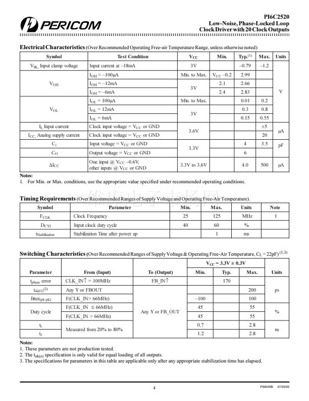
21098765432121098765432109876543210987654321210987654321098765432109876543212109876543210987654321098765432121098765432109876543210987654321
21098765432121098765432109876543210987654321210987654321098765432109876543212109876543210987654321098765432121098765432109876543210987654321
PI6C2520
Low-Noise Phase-Locked Loop
Clock Driver with 20 Clock Outputs
Product Features
聲 Low-Noise Phase-Locked Loop Clock Distribution.
聲 Allows Clock Input to have Spread Spectrum modulation
for EMI reduction. The clock outputs track the Clock Input
modulation.
聲 Maximum clock frequency of 125 MHz.
聲 Zero Input-to-Output delay.
聲 Low jitter: Cycle-to-Cycle jitter 鹵100ps max.
聲 On-chip series damping resistor at clock output drivers for
low noise and EMI reduction.
聲 Operates at 3.3V V
CC
.
聲 Output-to-Output skew less than 200ps.
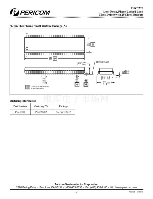
聲 Package: Plastic 56-pin TSSOP (A).
Product Description
The PI6C2520 is a low-skew, low-jitter, phase-locked loop (PLL)
clock driver, distributing low-noise clock signals for Networking
Applications. By connecting the feedback FB_OUT output to the
feedback FB_IN input, the propagation delay from the CLK_IN
input to any clock output will be nearly zero. This zero-delay
feature allows the CLK_IN input clock to be distributed, providing
5 banks of 4 clocks and an extra clock for feedback.
For test purposes, the PLL can be bypassed by strapping AV
CC
to
ground. The PI6C2520, which allows a Spread Spectrum clock in-
put, operates at 3.3V V
CC
and provides integrated series-damping
resistors that make it ideal for driving point-to-point loads. Output
signal duty cycles are adjusted to 50 percent, independent of the
duty cycle at the input clock.
Each bank of outputs can be enabled or disabled via the 1G, 2G,
3G, 4G, and 5G control inputs. When the G inputs are high, the
outputs switch in phase and frequency with CLK_IN. When the G
inputs are low, the outputs are disabled to the logic low state.
Product Pin Configuration
VCC
1Y0
1Y1
GND
GND
1Y2
1Y3
VCC
1G
GND
AVCC
CLK_IN
AGND
5G
GND
2G
VCC
2Y0
2Y1
GND
GND
2Y2
2Y3
VCC
VCC
5Y0
5Y1
GND
1
2
3
4
5
6
7
8
9
10
11
12
13
14
15
16
17
18
19
20
21
22
23
24
25
26
27
28
56
55
54
53
52
51
50
49
48
47
46
45
44
43
42
41
40
39
38
37
36
35
34
33
32
31
30
29
VCC
4Y0
4Y1
GND
GND
4Y2
4Y3
VCC
4G
GND
AVCC
FB_IN
AGND
FB_OUT
GND
3G
VCC
3Y0
3Y1
GND
GND
3Y2
3Y3
VCC
VCC
5Y3
5Y2
GND
Block Diagram
1G
2G
3G
4G
5G
4
4
4
4
1Y [0:3]
2Y [0:3]
3Y [0:3]
4Y [0:3]
56-Pin
A
CLK_IN
PLL
FB_IN
AVCC
4
5Y [0:3]
FB_OUT
1
PS8435B
07/25/00


 1
1
 2
2
 3
3
 4
4
 5
5
 6
6
