PIC18FX410/X490
Programming Specifications for
PIC18FX410/X490 FLASH MCUs
1.0
DEVICE OVERVIEW
2.1
Hardware Requirements
In High-Voltage ICSP mode, the PIC18FX410/X490
devices require two programmable power supplies:
one for V
DD
and one for MCLR/V
PP
. Both supplies
should have a minimum resolution of 0.25V. Refer to
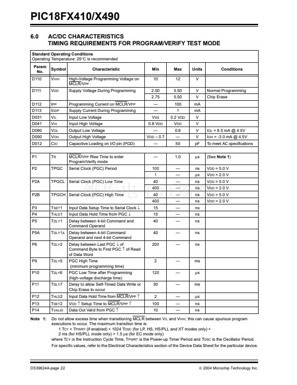
Section 6.0
鈥淎C/DC
Characteristics
Timing
Requirements for Program/Verify Test Mode鈥?/span>
for
additional hardware parameters.
This
document
includes
the
programming
specifications for the following devices:
鈥?PIC18F6410
鈥?PIC18F6490
鈥?PIC18F8410
鈥?PIC18F8490
2.0
PROGRAMMING OVERVIEW
OF THE PIC18FX410/X490
2.2
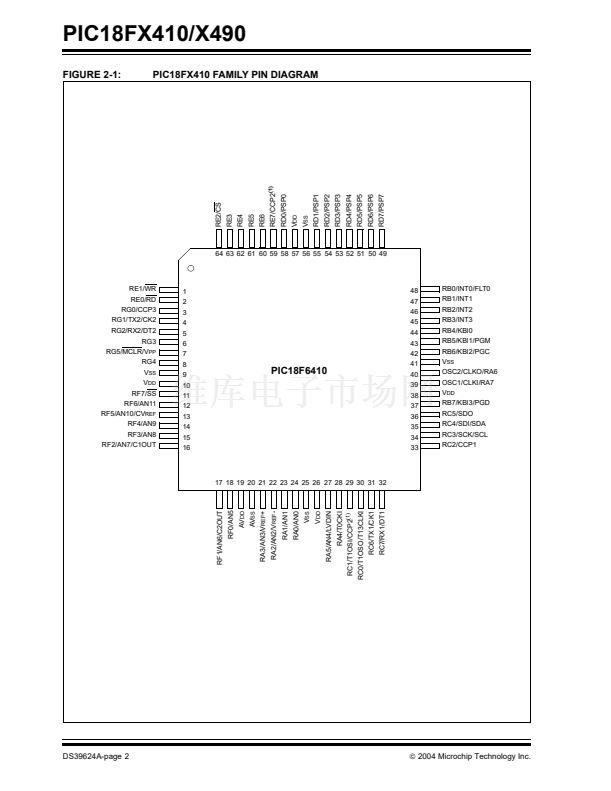
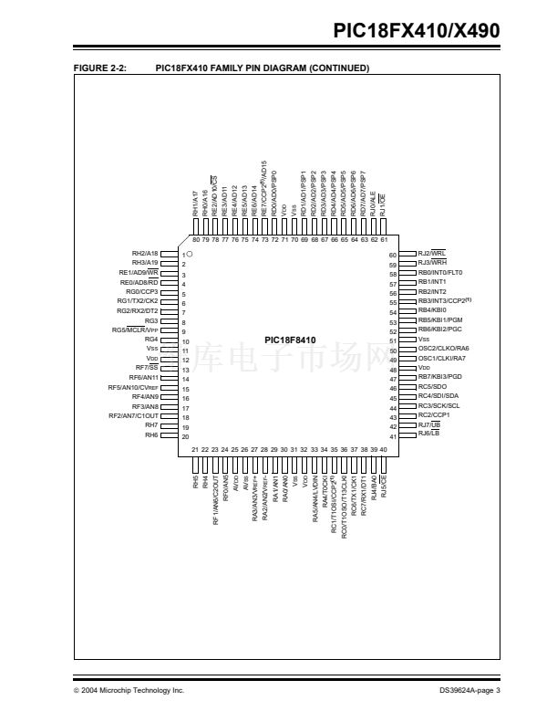
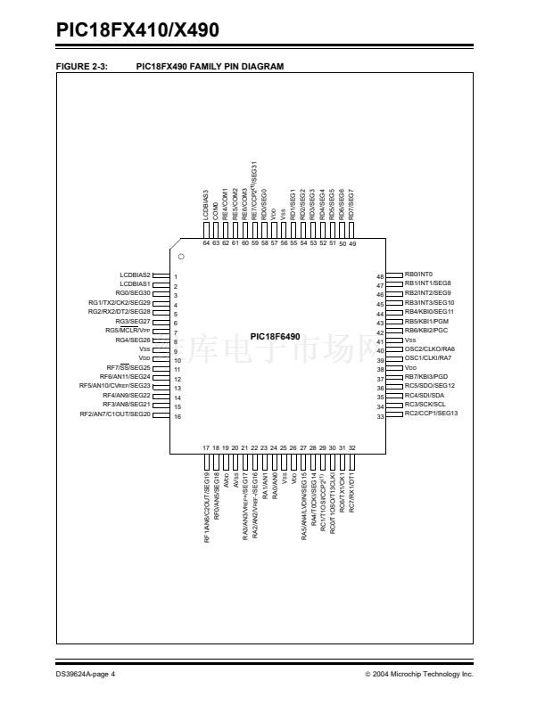
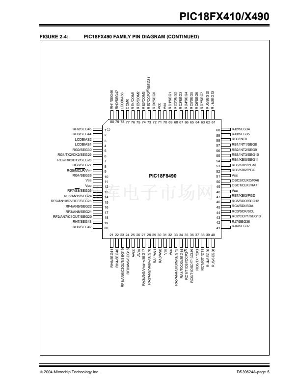
Pin Diagrams
PIC18FX410/X490 devices can be programmed using
the high-voltage In-Circuit Serial Programming
TM
(ICSP
TM
) method. This can be done with the device in
the user鈥檚 system. This programming specification
applies to PIC18FX410/X490 devices in all package
types.
The pin diagrams for the PIC18FX410/X490 family are
shown in Figure 2-1 through Figure 2-4.
TABLE 2-1:
Pin Name
PIN DESCRIPTIONS (DURING PROGRAMMING): PIC18FX410/X490
During Programming
Pin Name
Pin Type
P
P
P
I
I/O
Programming Enable
Power Supply
Ground
Serial Clock
Serial Data
Pin Description
RG5/MCLR/V
PP
V
DD
(1)
V
SS
(1)
RB6/PGC
RB7/PGD
V
PP
V
DD
V
SS
PGC
PGD
Legend:
I = Input, O = Output, P = Power
Note 1:
All power supply (V
DD
) and ground (V
SS
) must be connected.
錚?/div>
2004 Microchip Technology Inc.
DS39624A-page 1


 1
1
 2
2
 3
3
 4
4
 5
5
 6
6
 7
7
 8
8
 9
9
 10
10
 11
11
 12
12
 13
13
 14
14
 15
15
 16
16
 17
17
 18
18
 19
19
 20
20
 21
21
 22
22
 23
23
 24
24
