Powered by ICminer.com Electronic-Library Service CopyRight 2003
21098765432121098765432109876543210987654321210987654321098765432109876543212109876543210987654321098765432121098765432109876543210987654321
21098765432121098765432109876543210987654321210987654321098765432109876543212109876543210987654321098765432121098765432109876543210987654321
PI74AVC+16721
2.5V 20-Bit Flip-Flop
with 3-State Outputs
Product Features
聲
PI74AVC
+
16721 is designed for low voltage operation,
V
CC
= 1.65V to 3.6V
聲
True 鹵24mA Balanced Drive @ 3.3V
聲
I
OFF
supports partial power-down operation
聲
3.6V I/O Tolerant inputs and outputs
聲
All outputs contain noise reduction circuitry reducing
noise without speed degradation
聲 Industrial operation at 聳40擄C to +85擄C
聲 Available Packages:
聳 56-pin 240 mil wide plastic TSSOP (A)
聳 56-pin 173 mil wide plastic TVSOP (TSSOP) (K)
Product Description
Pericom Semiconductor聮s PI74AVC
+
series of logic circuits are
produced using the Company聮s advanced submicron CMOS
technology, achieving industry leading speed.
The PI74AVC
+
16721 is a 20-bit flip-flop with 3-state outputs
designed specifically for 1.65V to 3.6V V
CC
operation. The
device is designed with edge-triggered D-type flip-flops with
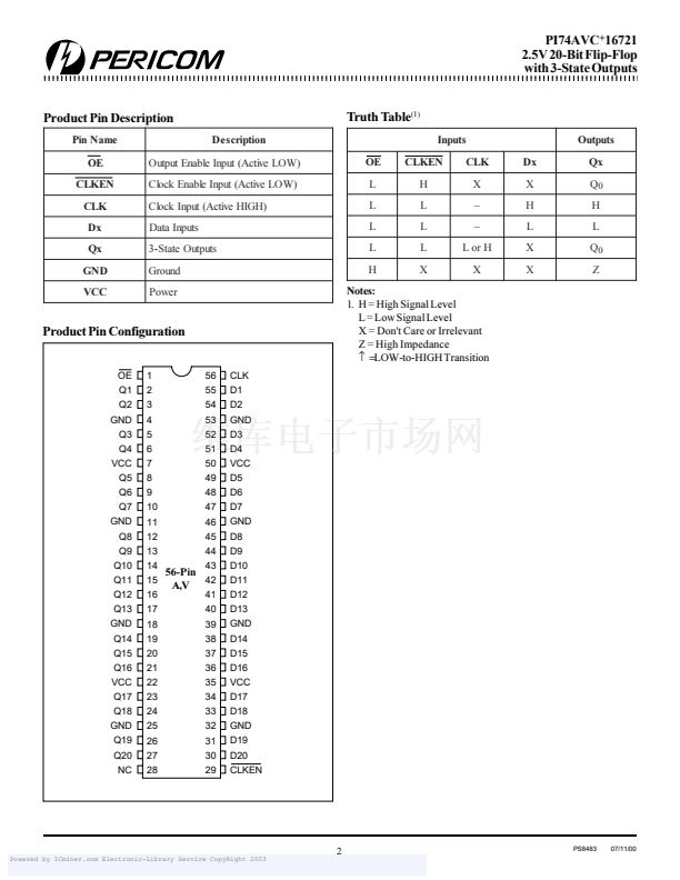
qualified clock storage. On the positive transition of clock (CLK)
input, the device provides true data at the Q outputs, provided
that the clock-enable (CLKEN) input is LOW. If CLKEN is HIGH,
no data is stored.
A buffered output-enable (OE) input can be used to place the
20 outputs in either a normal logic state (HIGH or LOW level) or a
high-impedance state. In the high-impedance state, the outputs
neither load nor drive the bus lines significantly. The high-impedance
state and increased drive provide the capacity to drive bus lines
without the need for interface or pullup components. OE does not
affect the internal operation of the flip-flops. Old data can be
retained or new data can be entered while the outputs are in the high-
impedance state.
To ensure the high-impedance state during power up or power
down, OE should be tied to V
CC
through a pullup resistor; the
minimum value of the resistor is determined by the current-sinking
capability of the driver.
Logic Block Diagram
1
56
29
2
55
1
PS8483
07/11/00


 1
1
 2
2
 3
3
 4
4
 5
5
 6
6
 7
7
 8
8
 9
9
 10
10
