V
V
21098765432121098765432109876543210987654321210987654321098765432109876543212109876543210987654321098765432121098765432109876543210987654321
21098765432121098765432109876543210987654321210987654321098765432109876543212109876543210987654321098765432121098765432109876543210987654321
PI74ALVTC16823
2.5V 18-Bit Bus Interface
Flip-Flop with 3-State Outputs
Product Features
聲 PI74ALVTC16823 is designed for low voltage operation,
V
DD
= 1.65V to 3.6V
聲 Supports Live Insertion
聲 3.6V I/O Tolerant Inputs and Outputs
聲 Bus Hold
聲 High Drive, 聳32/64mA @ 3.3V
聲 Uses patented noise reduction circuitry
聲 Power-off high impedance inputs and outputs
聲 Industrial operation at 聳40擄C to +85擄C
聲 Packages available:
聳 56-pin 240-mil wide plastic TSSOP (A56)
聳 56-pin 173-mil wide plastic TVSOP (K56)
Product Description
Pericom Semiconductor聮s PI74ALVTC series of logic circuits are
produced using the Company聮s advanced 0.35 micron CMOS
technology, achieving industry leading speed.
The PI74ALVTC16823 18-bit bus-interface flip-flop is designed for
1.65V to 3.6V V
CC
operation. It features 3-state outputs designed
specifically for driving highly capacitive or relatively low-impedance
loads. This device is particularly suitable for implementing wider
buffer registers, I/O ports, bidirectional bus drivers with parity, and
working registers.
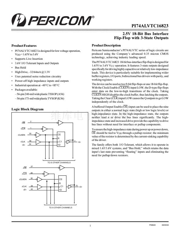
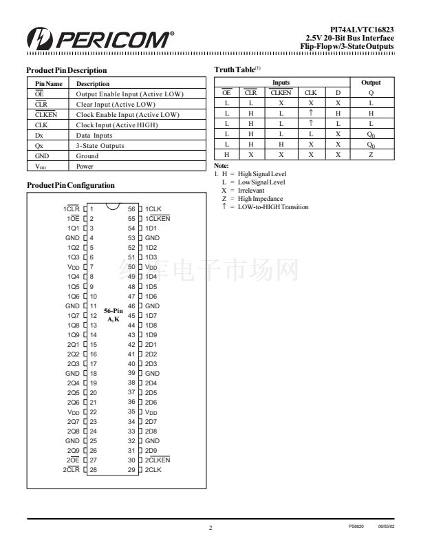
The device can be used as two 9-bit flip-flops or one 18-bit flip-flop.
With the Clock Enable (CLKEN) input LOW, the D-type flip-flops
enter data on the low-to-high transitions of the clock. Taking
CLKEN HIGH disables the clock buffer, thus latching the outputs.
Taking the Clear (CLR) input LOW causes the Q outputs to go LOW
independently of the clock.
A buffered Output Enable (OE) input can be used to place the nine
outputs in either a normal logic state (high or low logic levels) or
high-impedance state. In the high-impedance state, the outputs
neither load n or drive the bus lines significantly. The high-
impedance state and increased drive provide the capability to drive
bus lines without need for interface or pullup components.
To ensure the high-impedance state during power up or power down,
OE should be tied to V
DD
through a pullup resistor; the minimum
value of the resistor is determined by the current-sinking capability
of the driver.
The family offers both I/O Tolerant, which allows it to operate in
mixed 1.65/3.6V systems, and 聯(lián)Bus Hold,聰 which retains the data
input聮s last state preventing 聯(lián)floating聰 inputs and eliminating the
need for pullup/down resistors.
Logic Block Diagram
1
OE
2
1
CLR
1
55
1
CLKEN
CE
R
C1
3
1
Q
1
1
CLK
1
D
1
56
54
1D
TO 8 OTHER CHANNELS
2
OE
27
2
CLR
28
30
2
CLKEN
CE
R
C1
15
2
CLK
2
D
1
29
42
2
Q
1
1D
TO 8 OTHER CHANNELS
1
PS8620
06/05/02


 1
1
 2
2
 3
3
 4
4
 5
5
 6
6
 7
7
 8
8
