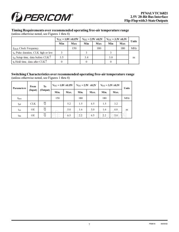
21098765432121098765432109876543210987654321210987654321098765432109876543212109876543210987654321098765432121098765432109876543210987654321
1
2109876543212109876543210987654321098765432121098765432109876543210987654321210987654321098765432109876543212109876543210987654321098765432
21098765432121098765432109876543210987654321210987654321098765432109876543212109876543210987654321098765432121098765432109876543210987654321
PI74ALVTC16821
Product Features
聲 PI74ALVTC16821 is designed for low voltage operation,
V
DD
= 1.65V to 3.6V
聲 Supports Live Insertion
聲 3.6V I/O Tolerant Inputs and Outputs
聲 Bus Hold
聲 High Drive, 聳32/64mA @ 3.3V
聲 Uses patented noise reduction circuitry
聲 Power-off high impedance inputs and outputs
聲 Industrial operation at 聳40擄C to +85擄C
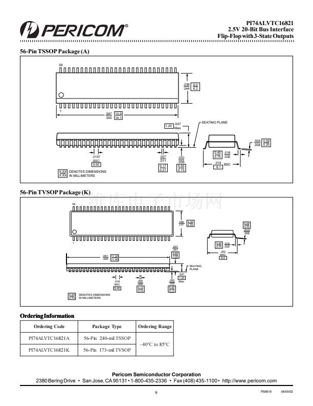
聲 Packages available:
聳 56-pin 240-mil wide plastic TSSOP (A56)
聳 56-pin 173-mil wide plastic TVSOP (K56)
2.5V 20-Bit Bus Interface
Flip-Flop with 3-State Outputs
Description
Pericom Semiconductor聮s PI74ALVTC series of logic circuits are
produced using the Company聮s advanced 0.35 micron CMOS
technology, achieving industry leading speed.
The PI74ALVTC16821is a 20-bit bus interface flip-flop designed for
1.65V to 3.6V V
CC
operation. It can be used as two 10-bit flip-flops
or one 20-bit flip-flop. The 20 flip-flops are edge-triggered D-type
flip-flops. On the positive transition of the clock (CLK) input, the
device provides true data at the Q outputs.
A buffered output-enable (OE) input can be used to place the ten
outputs in either a normal logic state (HIGH or LOW level) or a high-
impedance state. In the high-impedance state, the outputs neither
load nor drive the bus lines significantly. The high-impedance state
and increased drive provide the capacity to drive bus lines without
the need for interface or pullup components.
OE does not affect the internal operation of the flip-flops. Old data
can be retained or new data can be entered while the outputs are in
the high-impedance state.
To ensure the high-impedance state during power up or power
down, OE should be tied to V
CC
through a pullup resistor; the
minimum value of the resistor is determined by the current sinking
capability of the driver.
The family offers both I/O Tolerant, which allows it to operate in
mixed 1.65/3.6V systems, and 聯(lián)Bus Hold,聰 which retains the data
input聮s last state preventing 聯(lián)floating聰 inputs and eliminating the
need for pullup/down resistors.
Logic Block Diagram
1
OE
1
2
OE
28
1CLK 56
One of Ten
Channels
2CLK 29
One of Ten
Channels
1
Q
1
C
1
1
D
1D
1
55
2
C
1
1
D
2D
1
42
15
2Q
1
TO 9 OTHER CHANNELS
TO 9 OTHER CHANNELS
1
PS8618
06/05/02


 1
1
 2
2
 3
3
 4
4
 5
5
 6
6
 7
7
 8
8
 9
9
