21098765432121098765432109876543210987654321210987654321098765432109876543212109876543210987654321098765432121098765432109876543210987654321
21098765432121098765432109876543210987654321210987654321098765432109876543212109876543210987654321098765432121098765432109876543210987654321
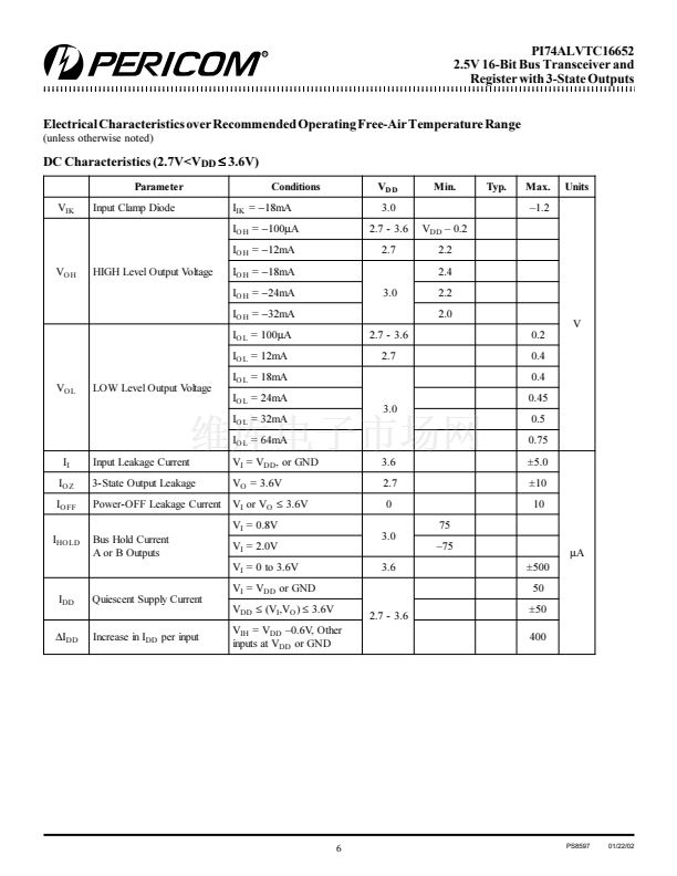
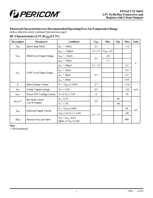
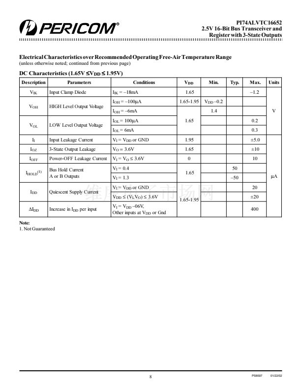
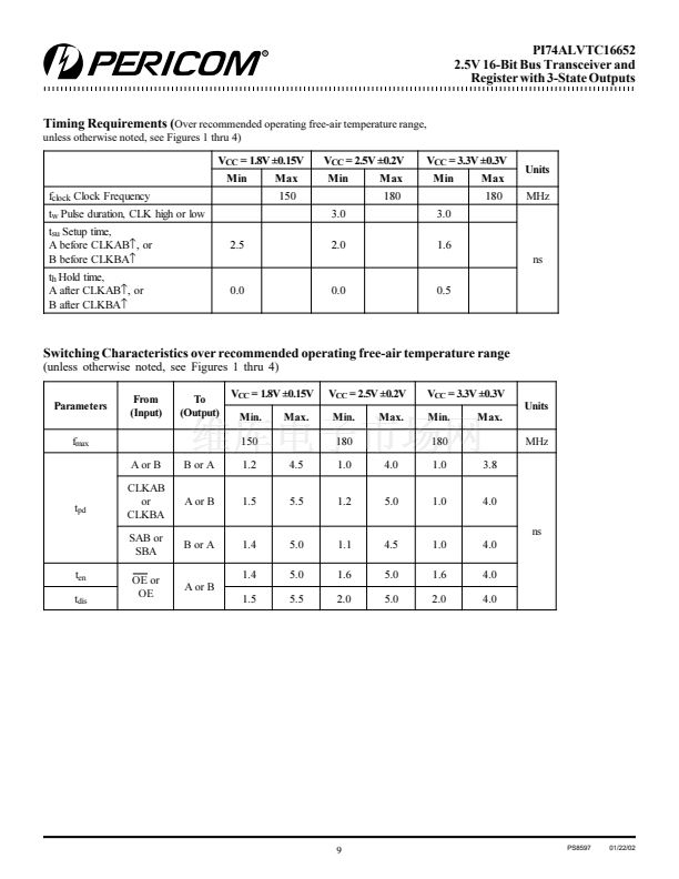
PI74ALVTC16652
2.5V 16-Bit Bus Transceiver and
Register with 3-State Outputs
Product Features
聲 PI74ALVTC16652 is designed for low voltage operation,
V
DD
= 1.65V to 3.6V
聲 Supports Live Insertion
聲 3.6V I/O Tolerant Inputs and Outputs
聲 Bus Hold
聲 High Drive, 聳32/64mA @ 3.3V
聲 Uses patented noise reduction circuitry
聲 Power-off high impedance inputs and outputs
聲 Industrial operation at 聳40擄C to +85擄C
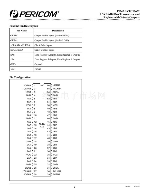
聲 Packages available:
聳 56-pin 240-mil wide plastic TSSOP (A56)
聳 56-pin 173-mil wide plastic TVSOP (K56)
Product Description
Pericom Semiconductor聮s PI74ALVTC series of logic circuits are
produced using the Company聮s advanced 0.35 micron CMOS
technology, achieving industry leading speed.
The PI74ALVTC16652 is a 16-bit bus transceiver and register designed
for low 1.65V to 3.6V Vcc operation. It consists of D-type flip-flops
and control circuitry arranged for multiplexed transmission of data
directly from the data bus or from the internal storage registers. The
device can be used as two 8-bit transceivers or one 16-bit transceiver.
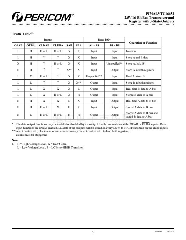
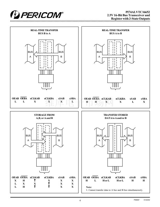
Complementary Output Enable (OEAB and OEBA) inputs are
provided to control the transceiver functions. Select Control (SAB
and SBA) inputs are provided to select whether real-time or stored
data is transferred. A low input level selects real-time data, and a high
input level selects stored data. Circuitry used for Select Control
eliminates the typical decoding glitch that occurs in a multiplexer
during the transition between stored and real-time data.
Data on the A or B bus, or both, can be stored in the internal D flip-
flops by low-to-high transitions at the appropriate clock (CLKAB or
CLKBA) inputs regardless of the levels on the Select Control or
Output Enable inputs. When SAB and SBA are in the real-time
transfer mode, it also is possible to store data without using the
internal D-type flip-lops by simultaneously enabling OEAB and
OEBA. In this configuration, each output reinforces its input. Thus,
when all other data sources to the two sets of bus lines are in the high-
impedance state, each set of bus lines remains at its last level
configuration.
To ensure the high-impedance state during power up or power down,
OEBA should be tied to Vcc through a pull-up resistor and OEAB
should be tied to GND through a pull-down resistor; the minimum
value of the resistor is determined by the current-sinking current
sourcing capability of the driver.
The family offers both I/O Tolerant, which allows it to operate in
mixed 1.65/3.6V systems, and 聯(lián)Bus Hold,聰 which retains the data
input聮s last state preventing 聯(lián)floating聰 inputs and eliminating the
need for pullup/down resistors.
Logic Block Diagram
1OEBA 56
1
55
1OEAB
1CLKBA
1SBA 54
1CLKAB
1SAB
2
3
One of Eight Channels
1D
C1
1A1
5
52
1D
C1
1B1
TO SEVEN OTHER CHANNELS
2OEBA 29
28
30
2OEAB
2CLKBA
2SBA 31
2CLKAB 27
2SAB 26
One of Eight Channels
1D
C1
2A1
15
42
1D
C1
2B1
TO SEVEN OTHER CHANNELS
1
PS8597
01/22/02


 1
1
 2
2
 3
3
 4
4
 5
5
 6
6
 7
7
 8
8
 9
9
 10
10
 11
11
