21098765432121098765432109876543210987654321210987654321098765432109876543212109876543210987654321098765432121098765432109876543210987654321
21098765432121098765432109876543210987654321210987654321098765432109876543212109876543210987654321098765432121098765432109876543210987654321
PI74ALVTC16646
2.5V 16-Bit Bus Transceiver and
Register with 3-State Outputs
Product Features
聲 PI74ALVTC16646 is designed for low voltage operation,
V
DD
= 1.65V to 3.6V
聲 Supports Live Insertion
聲 3.6V I/O Tolerant Inputs and Outputs
聲 Bus Hold
聲 High Drive, 聳32/64mA @ 3.3V
聲 Uses patented noise reduction circuitry
聲 Power-off high impedance inputs and outputs
聲 Industrial operation at 聳40擄C to +85擄C
聲 Packages available:
聳 56-pin 240-mil wide plastic TSSOP (A56)
聳 56-pin 173-mil wide plastic TVSOP (K56)
Product Description
Pericom Semiconductor聮s PI74ALVTC series of logic circuits are
produced using the Company聮s advanced 0.35 micron CMOS
technology, achieving industry leading speed.
The PI74ALVTC16646 is a 16-bit bus transceiver and register
designed for 1.65V to 3.6V V
CC
operation. It can be used as two 8-
bit transceivers or one 16-bit transceiver. Data on the A or B bus is
clocked into the registers on the low-to-high transition of the
appropriate Clock (CLKAB or CLKBA) input. Four fundamental
bus-management functions can be performed.
Output Enable (OE) and Direction Control (DIR) inputs are provided
to control the transceiver functions. In the transceiver mode, data
present at the high-impedance port may be stored in either register
or in both. The Select Control (SAB and SBA) inputs can multiplex
stored and real-time (transparent mode) data. Circuitry used for
Select Control eliminates the typical decoding glitch that occurs in
a multiplexer during the transition between stored and real-time
data. DIR determines which bus receives data when OE is LOW. In
the isolation mode (OE HIGH), A data may be stored in one register
and/or B data may be stored in the other register.
When an output function is disabled, the input function is still
enabled and may be used to store and transmit data. Only one of the
two buses, A or B, can be driven at a time.
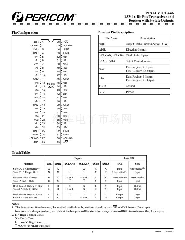
Logic Block Diagrams
1OE 56
1DIR
1CLKBA
1
55
1SBA 54
1CLKAB
1SAB
2
3
One of Eight Channels
1D
C1
1A1
5
52
1D
C1
1B1
To ensure the high-impedance state during power up or power
down, OE should be tied to V
CC
through a pullup resistor; the
minimum value of the resistor is determined by the current-sinking
capability of the driver.
Active bus-hold circuitry is provided to hold unused or floating
data inputs at a valid logic level.
The family offers both I/O Tolerant, which allows it to operate in
mixed 1.65/3.6V systems, and 聯(lián)Bus Hold,聰 which retains the data
input聮s last state preventing 聯(lián)floating聰 inputs and eliminating the
need for pullup/down resistors.
TO SEVEN OTHER CHANNELS
2OE
2DIR
2CLKBA
2SBA
2CLKAB
2SAB
29
28
30
31
27
26
One of Eight Channels
1D
C1
42
2B1
2A115
1D
C1
TO SEVEN OTHER CHANNELS
1
PS8596
01/22/02


 1
1
 2
2
 3
3
 4
4
 5
5
 6
6
 7
7
 8
8
 9
9
