21098765432121098765432109876543210987654321210987654321098765432109876543212109876543210987654321098765432121098765432109876543210987654321
21098765432121098765432109876543210987654321210987654321098765432109876543212109876543210987654321098765432121098765432109876543210987654321
PI74ALVTC16601
2.5V, 18-Bit Universal Bus Transceiver
with 3-State Outputs
Product Features
聲 PI74ALVTC16601 is designed for low voltage operation,
V
DD
= 1.65V to 3.6V
聲 Supports Live Insertion
聲 3.6V I/O Tolerant Inputs and Outputs
聲 Bus Hold
聲 High Drive, 聳32/64mA @ 3.3V
聲 Uses patented noise reduction circuitry
聲 Power-off high impedance inputs and outputs
聲 Industrial operation at 聳40擄C to +85擄C
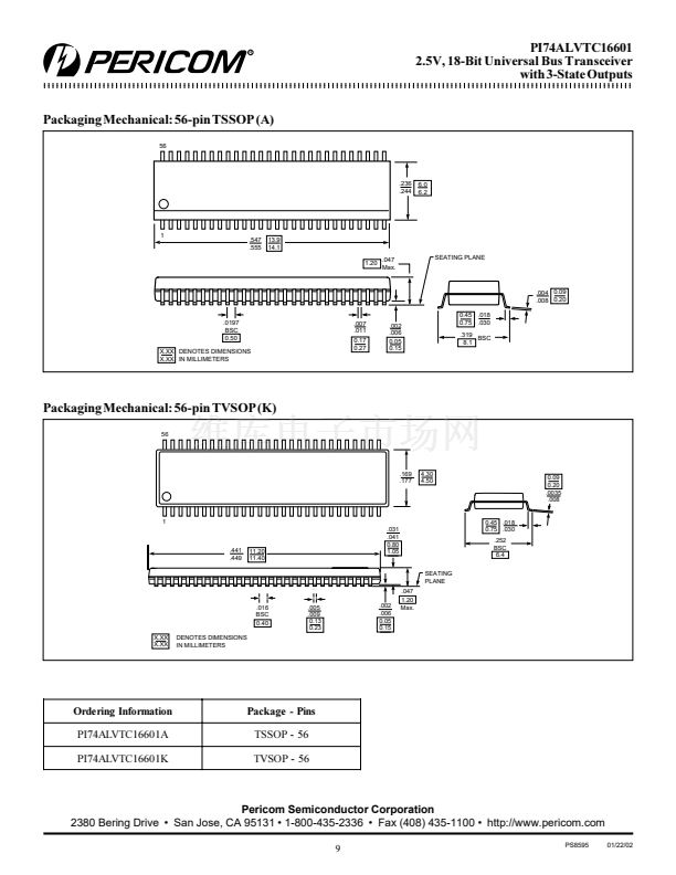
聲 Packages available:
聳 56-pin 240-mil wide plastic TSSOP (A56)
聳 56-pin 173-mil wide plastic TVSOP (K56)
Product Description
Pericom Semiconductor聮s PI74ALVTC series of logic circuits are
produced using the Company聮s advanced 0.35 micron CMOS
technology, achieving industry leading speed.
The PI74ALVTC16601 uses D-type latches and D-type flip-flops
with 3-state outputs to allow data flow in transparent, latched, and
clocked modes.
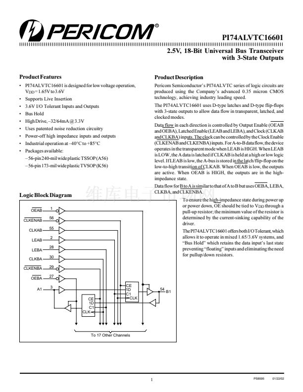
Data flow in each direction is controlled by Output Enable (OEAB
and OEBA), Latched Enable (LEAB and LEBA), and Clock (CLKAB
and CLKBA) inputs. The clock can be controlled by the Clock Enable
(CLKENAB and CLKENBA) inputs. For A-to-B data flow, the device
operates in the transparent mode when LEAB is HIGH. When LEAB
is LOW, the A data is latched if CLKAB is held at a high or low logic
level. If LEAB is low, the A-bus is stored in the latch/flip-flop on the
low-to-high transition of CLKAB. When OEAB is low, the outputs
are active. When OEAB is HIGH, the outputs are in the high-
impedance state.
Data flow for B to A is similar to that of A to B but uses OEBA, LEBA,
CLKBA, and CLKENBA.
To ensure the high-impedance state during power up
or power down, OE should be tied to V
DD
through a
pull-up resistor; the minimum value of the resistor is
determined by the current-sinking capability of the
driver.
The PI74ALVTC16601 offers both I/O Tolerant, which
allows it to operate in mixed 1.65/3.6V systems, and
聯(lián)Bus Hold聰 which retains the data input聮s last state
preventing 聯(lián)floating聰 inputs and eliminating the need
for pullup/down resistors.
Logic Block Diagram
OEAB
CLKENAB
CLKAB
LEAB
LEBA
CLKBA
CLKENBA
OEBA
A1
1
56
55
2
28
30
29
27
3
CE
1D
C1
CLK
CE
1D
C1
CLK
54
B1
To 17 Other Channels
1
PS8595
01/22/02


 1
1
 2
2
 3
3
 4
4
 5
5
 6
6
 7
7
 8
8
 9
9
