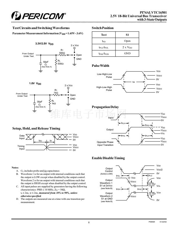
21098765432121098765432109876543210987654321210987654321098765432109876543212109876543210987654321098765432121098765432109876543210987654321
21098765432121098765432109876543210987654321210987654321098765432109876543212109876543210987654321098765432121098765432109876543210987654321
21098765432121098765432109876543210987654321210987654321098765432109876543212109876543210987654321098765432121098765432109876543210987654321
PI74ALVTC16501
2.5V 18-Bit Universal Bus Transceiver
With 3-State Outputs
Product Description
Product Features
聲 PI74ALVTC16501 is designed for low voltage operation,
V
DD
= 1.65V to 3.6V
聲 Supports Live Insertion
聲 3.6V I/O Tolerant Inputs and Outputs
聲 Bus Hold
聲 High Drive, 聳32/64mA @ 3.3V
聲 Uses patented noise reduction circuitry
聲 Power-off high impedance inputs and outputs
聲 Industrial operation at 聳40擄C to +85擄C
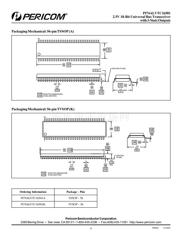
聲 Packages available:
聳 56-pin 240-mil wide plastic TSSOP (A)
聳 56-pin 173-mil wide plastic TVSOP (K)
Pericom Semiconductor聮s PI74ALVTC series of logic
circuits are produced using the Company聮s advanced
0.35 micron CMOS technology, achieving industry
leading speed.
The 18-bit PI74ALVTC16501 univeral bus transceiver
is designed for 1.65V to 3.6V V
DD
operation.
Data flow in each direction is controlled by Output
Enable (OEAB and OEBA), Latch Enable (LEAB and
LEBA), and CLOCK (CLKAB and CLKBA) inputs. For
A-to-B data flow, the device operates in the transparent
mode when LEAB is HIGH. When LEAB is LOW, the
A data is latched if CLKAB is held at a high or low logic
level. If LEAB is LOW, the A-bus data is stored in the
latch/flip-flop on the low-to-high transition of CLKAB.
When OEAB is HIGH, the outputs are active. When
OEAB is LOW, the outputs are in the high-impedance
state.
Data flow for B to A is similar to that of A to B but uses
OEBA, LEBA, and CLKBA. The Output Enables are
complementary (OEAB is active HIGH and OEBA is
active LOW)
To ensure the high-impedance state during power up
or power down, OEBA should be tied to V
DD
through
a pull-up resistor and OEAB should be tied to GND
through a pulldown resistor; the minimum value of the
resistor is determined by the current-sinking capability
of the driver.
Logic Block Diagram
1
PS8594
01/22/02


 1
1
 2
2
 3
3
 4
4
 5
5
 6
6
 7
7
 8
8
 9
9
