21098765432121098765432109876543210987654321210987654321098765432109876543212109876543210987654321098765432121098765432109876543210987654321
21098765432121098765432109876543210987654321210987654321098765432109876543212109876543210987654321098765432121098765432109876543210987654321
21098765432121098765432109876543210987654321210987654321098765432109876543212109876543210987654321098765432121098765432109876543210987654321
PI74ALVCH16820
3.3V 10-Bit Flip-Flop with Dual Outputs
and 3-State Outputs
Product Features
聲 PI74ALVCH16820 is designed for low-voltage operation
聲 V
CC
= 2.3V to 3.6V
聲 Hysteresis on all inputs
聲 Typical V
OLP
(Output Ground Bounce) < 0.8V
at V
CC
= 3.3V, T
A
= 25擄C
聲 Typical V
OHV
(Output V
OH
Undershoot) < 2.0V
at V
CC
= 3.3V, T
A
= 25擄C
聲 Bus Hold retains last active bus state during 3-state
eliminating the need for external pullup resistors
聲 Industrial operation: 聳40擄C to +85擄C
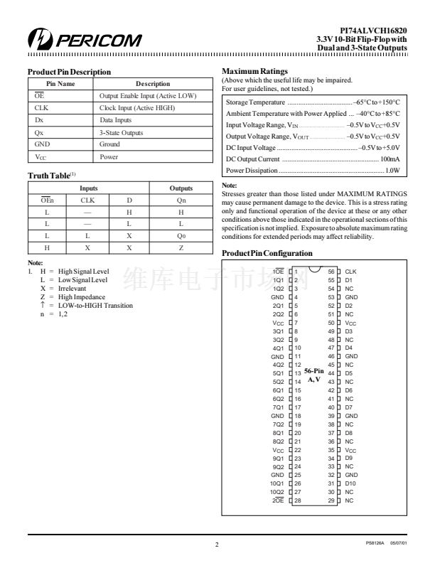
聲 Packages available:
聳 56-pin 240 mil wide plastic TSSOP (A)
聳 56-pin 300 mil wide plastic SSOP (V)
Product Description
Pericom Semiconductor聮s PI74ALVCH series of logic circuits are
produced using the Company聮s advanced 0.5 micron CMOS
technology, achieving industry leading speed.
The PI74ALVCH16820, a 10-bit flip-flop designed for 2.3V to 3.3V
V
CC
operation, features edge-triggered D-type flip-flops. On the
positive transition of clock (CLK) input, the device provides true
data at the Q outputs.
A buffered output-enable (OE) input can be used to place the ten
outputs in either a normal logic state (HIGH or LOW level) or a high-
impedance state. In high-impedance state, outputs neither load nor
drive the bus lines significantly. The high-impedance state and
increased drive are able to drive bus lines without interface or pullup
components.
OE does not affect the internal operation of the flip-flops. Old data
can be retained or new data can be entered while the outputs are in
the high-impedance state.
To ensure the high-impedance state during power up or power
down, OE should be tied to V
CC
through a pullup resistor whose
minimum value is determined by the current sinking capability of the
driver.
To prevent 聯(lián)floating聰 inputs and to eliminate the need for pullup/
down resistors, the PI74ALVCH16820 has 聯(lián)Bus Hold聰 which retains
the data input聮s last state whenever the data input goes to high-
impedance .
Active bus-hold circuitry is provided to hold unused or floating
data inputs at a valid logic level.
Logic Block Diagram
1
OE
1
2
OE
28
2
C
1
1
D
CLK
56
55
1
Q
1
D
1
3
1
Q
2
TO 9 OTHER CHANNELS
1
PS8126A
05/07/01


 1
1
 2
2
 3
3
 4
4
