鈥?/div>
PI74ALVCH16601 is designed for low voltage operation
V
CC
= 2.3V to 3.6V
Hysteresis on all inputs
Typical V
OLP
(Output Ground Bounce)
< 0.8V at V
CC
= 3.3V, T
A
= 25擄C
Typical V
OHV
(Output V
OH
Undershoot)
< 2.0V at V
CC
= 3.3V, T
A
= 25擄C
Bus Hold retains last active bus state during 3-State,
eliminating the need for external pullup resistors
Industrial operation at 聳40擄C to +85擄C
Packages available:
聳 56-pin 240 mil wide plastic TSSOP (A)
聳 56-pin 300 mil wide plastic SSOP (V)
Product Description
Pericom Semiconductor聮s PI74ALVCH series of logic
circuits are produced using the Company聮s advanced
0.5 micron CMOS technology, achieving industry
leading speed.
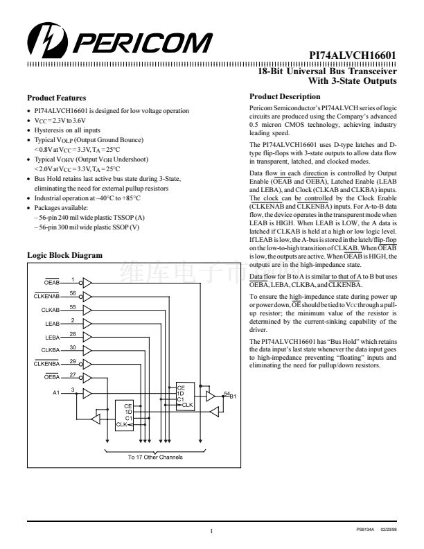
The PI74ALVCH16601 uses D-type latches and D-
type flip-flops with 3-state outputs to allow data flow
in transparent, latched, and clocked modes.
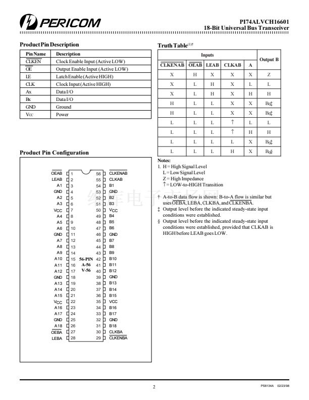
Data flow in each direction is controlled by Output
Enable (OEAB and OEBA), Latched Enable (LEAB
and LEBA), and Clock (CLKAB and CLKBA) inputs.
The clock can be controlled by the Clock Enable
(CLKENAB and CLKENBA) inputs. For A-to-B data
flow, the device operates in the transparent mode when
LEAB is HIGH. When LEAB is LOW, the A data is
latched if CLKAB is held at a high or low logic level.
If LEAB is low, the A-bus is stored in the latch/flip-flop
on the low-to-high transition of CLKAB. When OEAB
is low, the outputs are active. When OEAB is HIGH, the
outputs are in the high-impedance state.
Data flow for B to A is similar to that of A to B but uses
OEBA, LEBA, CLKBA, and CLKENBA.
To ensure the high-impedance state during power up
or power down, OE should be tied to V
CC
through a pull-
up resistor; the minimum value of the resistor is
determined by the current-sinking capability of the
driver.
The PI74ALVCH16601 has 聯(lián)Bus Hold聰 which retains
the data input聮s last state whenever the data input goes
to high-impedance preventing 聯(lián)floating聰 inputs and
eliminating the need for pullup/down resistors.
Logic Block Diagram
1
PS8134A
02/23/98


 1
1
 2
2
 3
3
 4
4
 5
5
