鈥?/div>
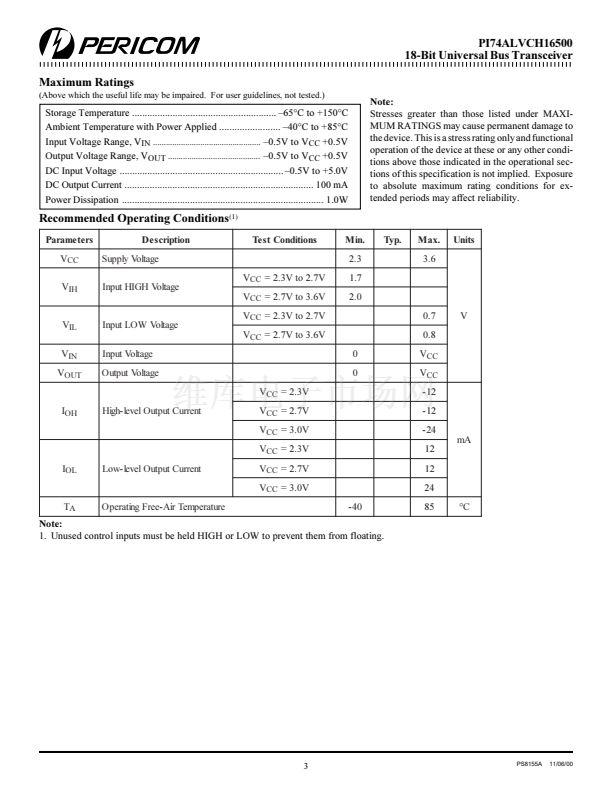
PI74ALVCH16500 is designed for low voltage operation
V
CC
= 2.3V to 3.6V
Hysteresis on all inputs
Typical V
OLP
(Output Ground Bounce)
< 0.8V at V
CC
= 3.3V, T
A
= 25擄C
Typical V
OHV
(Output V
OH
Undershoot)
< 2.0V at V
CC
= 3.3V, T
A
= 25擄C
Bus Hold retains last active bus state during 3-State
eliminating the need for external pullup resistors
Industrial operation at 聳40擄C to +85擄C
Packages available:
聳 56-pin 240 mil wide plastic TSSOP (A)
聳 56-pin 300 mil wide plastic SSOP (V)
Product Description
Pericom Semiconductor聮s PI74ALVCH series of logic circuits are
produced using the Company聮s advanced 0.5 micron CMOS
technology, achieving industry leading speed.
The 18-bit PI74ALVCH16500 univeral bus transceiver is designed
for 2.3V to 3.6V Vcc operation.
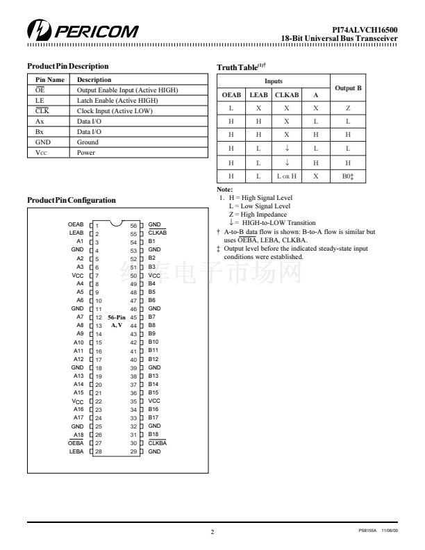
Data flow in each direction is controlled by Output Enable (OEAB
and OEBA), Latch- Enable (LEAB and LEBA), and clock (CLKAB
and CLKBA) inputs. For A- to-B data flow, the device operates in
the transparent mode when LEAB is high. When LEAB is low, the
A data is latched if CLKAB is held at a high or low logic level. If
LEAB is low, the A data is stored in the latch/flip-flop on the high-
to-low transition of CLKAB. Output-enable OEAB is active high.
When OEAB is high, the B-port outputs are active. When OEAB is
low, the B-port outputs are in the high-impedence state.
Data flow for B to A is similar to that of A to B but uses OEBA,
LEBA, and CLKBA. The Output Enables are complementary
(OEAB is active HIGH and OEBA is active LOW).
To ensure the high-impedance state during power up or power
down, OEBA should be tied to Vcc through a pull-up resistor and
OEAB should be tied to GND through a pulldown resistor; the
minimum value of the resistor is determined by the current-sinking/
current-sourcing capability of the driver.
Active bus-hold circuitry is provided to hold unused or floating
data inputs at a valid logic level.
Logic Block Diagram
OEAB
1
CLKAB
55
2
LEAB
28
LEBA
CLKBA
30
27
OEBA
3
A1
1D
C1
CLK
C1 1D
C1
1D
CLK
54
B1
TO 17 OTHER CHANNELS
1
PS8155A
11/06/00


 1
1
 2
2
 3
3
 4
4
 5
5
