21098765432121098765432109876543210987654321210987654321098765432109876543212109876543210987654321098765432121098765432109876543210987654321
21098765432121098765432109876543210987654321210987654321098765432109876543212109876543210987654321098765432121098765432109876543210987654321
PI74ALVC162834F
18-Bit Universal Bus Driver
with 3-State Outputs
Product Features
鈥?PI74ALVC162834F is designed for low voltage operation,
V
CC
= 2.3V to 3.6V
鈥?Outputs have equivalent 26 -Ohm series resistors
鈥?Supports PC133 Registered DIMM
鈥?Typical V
OLP
(Output Ground Bounce)
< 0.8V at V
CC
= 3.3V, T
A
= 25擄C
鈥?Typical V
OHV
(Output Voh Undershoot)
< 2.0V at V
CC
= 3.3V, T
A
= 25擄C
鈥?Industrial operation at 鈥?0擄C to +85擄C
鈥?Packages available:
- 56-pin 240 mil wide plastic TSSOP (A)
- Pb-free, 56-pin 240 mil wide plastic TSSOP (AE)
- 56-pin 173 mil wide plastic TVSOP (K)
- 56-pin 300 mil wide plastic SSOP (V)
Product Description
Pericom Semiconductor鈥檚 PI74ALVC series of logic circuits
are produced using the Company鈥檚 advanced 0.5 micron CMOS
technology, achieving industry leading speed.
The 18-bit PI74ALVC162834F universal bus driver is designed
for 2.3V to 3.6V V
CC
operation.
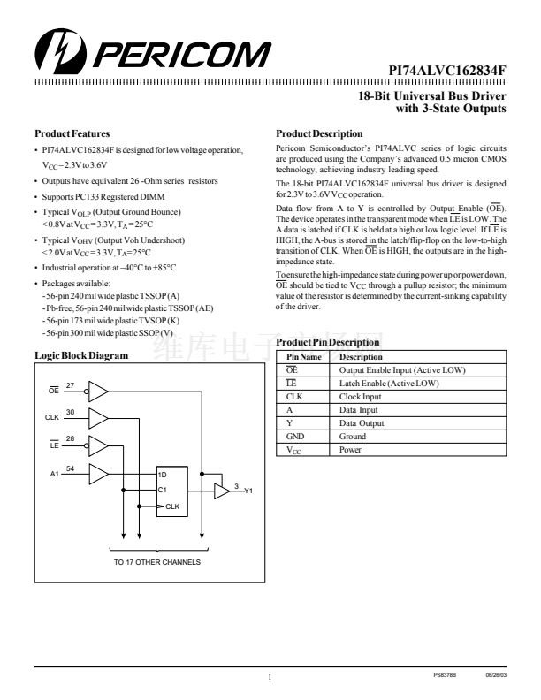
Data flow from A to Y is controlled by Output Enable (OE).
The device operates in the transparent mode when LE is LOW. The
A data is latched if CLK is held at a high or low logic level. If LE is
HIGH, the A-bus is stored in the latch/flip-flop on the low-to-high
transition of CLK. When OE is HIGH, the outputs are in the high-
impedance state.
To ensure the high-impedance state during power up or power down,
OE should be tied to V
CC
through a pullup resistor; the minimum
value of the resistor is determined by the current-sinking capability
of the driver.
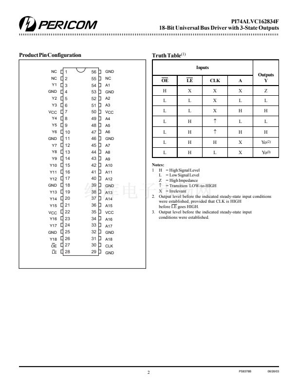
Product Pin Description
Pin Name
OE
LE
CLK
A
Y
GND
V
CC
Description
Output Enable Input (Active LOW)
Latch Enable (Active LOW)
Clock Input
Data Input
Data Output
Ground
Power
Logic Block Diagram
27
OE
CLK
30
28
LE
54
A1
1D
C1
CLK
3
Y1
TO 17 OTHER CHANNELS
1
PS8378B
06/26/03


 1
1
 2
2
 3
3
 4
4
 5
5
 6
6
