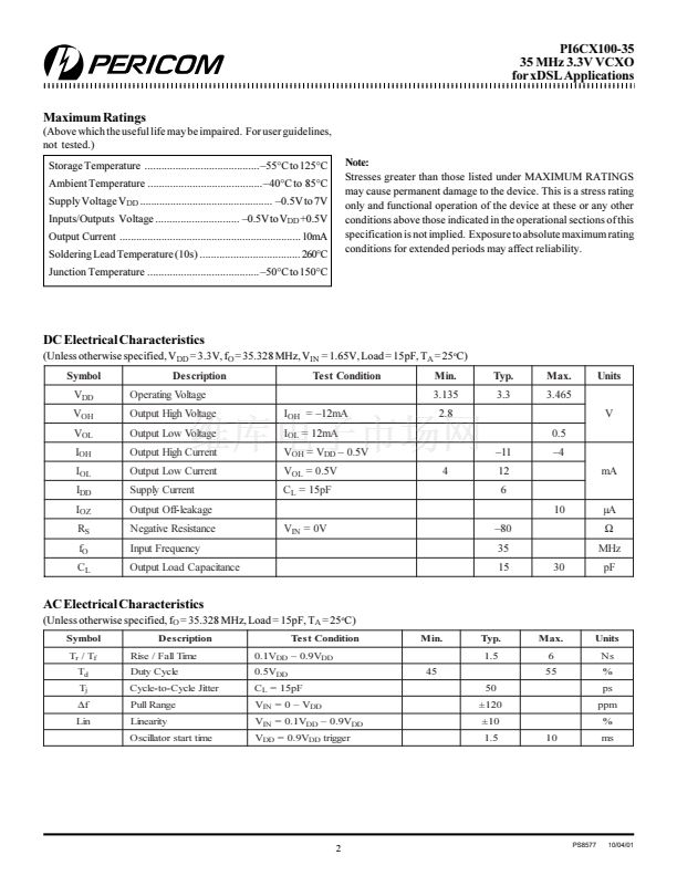
21098765432121098765432109876543210987654321210987654321098765432109876543212109876543210987654321098765432121098765432109876543210987654321
21098765432121098765432109876543210987654321210987654321098765432109876543212109876543210987654321098765432121098765432109876543210987654321
21098765432121098765432109876543210987654321210987654321098765432109876543212109876543210987654321098765432121098765432109876543210987654321
PI6CX100-35
35 MHz 3.3V VCXO
for xDSL Applications
Product Features
聲
3.3V operating voltage
聲
Uses an inexpensive external crystal
聲
On-chip VCXO with pull range of 240ppm
聲
VCXO tuning voltage from 0 to 3.3V
聲
10mA output drive at CMOS levels
聲
Available in SOIC package
Product Description
The PI6CX100-35 is a low-cost, high-performance 3.3V VCXO,
designed to replace expensive VCXO modules. The on-chip Voltage
Controlled Crystal Oscillator accepts a 0 to 3.3V input voltage to
cause clocks to vary by
鹵120ppm.
This device uses an inexpensive
external pullable crystal at 35 MHz to produce the same output
frequency.
The PI6CX100-35 is designed for xDSL applications.
Logic Block Diagram
V
IN
Product Pin Configuration
X1
Output
Buffer
Voltage
Controlled
Crystal
Oscillator
CLKOUT
1
W
8
X2
NC
VDD
CLKOUT
NC
VIN
GND
2
8-Pin
7
3
4
6
5
X1
X2
Pin Description
Pin Name
X1, X2
NC
V
IN
GND
CLKOUT
V
DD
Note:
1. 0.1碌F or 0.01碌F bypass capacitor is required.
Pin Numbe r
1, 8
2, 7
3
4
5
6
Type
I
I
PWR
O
PWR
De s cription
Crystal Connection
No Connect
Voltage Input to VCXO
Ground
Clock Output
Power Supply
(1)
1
PS8577
10/04/01


 1
1
 2
2
 3
3
 4
4
