21098765432121098765432109876543210987654321210987654321098765432109876543212109876543210987654321098765432121098765432109876543210987654321
21098765432121098765432109876543210987654321210987654321098765432109876543212109876543210987654321098765432121098765432109876543210987654321
PI6CV850
2.5-V Phase Lock Loop Clock Driver
with I
2
C Control Interface
Features
聲 Phase-Lock Loop Clock Driver for Double Data Rate
Synchronous DRAM Applications
聲 Spread Spectrum Clock Compatible
聲 Operating Frequency: 60 to 170 MHz
聲 Low Jitter (cycle-cycle): <|75ps|
聲 Distributes One Differential Clock Input to Ten
Differential Outputs
聲 I
2
C Serial Interface Provides Output Enable and
Functional Control
聲 Three-State Outputs when I
2
C low-level control
bit is written
聲 Operates from dual 2.5-V and 3.3 V Supplies
聲 External Feedback Pins (FBIN,FBIN) are used to
Synchronize the Outputs to the Input Clocks
聲 Low Jitter < 100ps
聲 Low Skew < 100ps
聲 Low Phase Offset: TBD
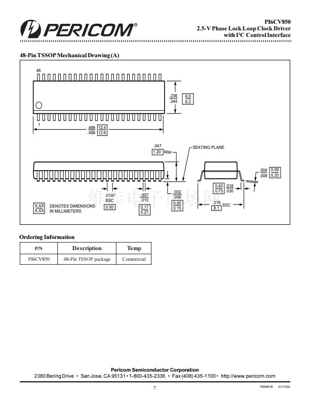
聲 48-Pin TSSOP Package
Description
PI6CV850 is a high-performance, low-skew, low-jitter zero-delay buffer
that distributes a differential clock input pair (CLK, CLK) to ten
differential pair of clock outputs (Y[0:9], Y[0:9]) and one differential pair
feedback clock output (FBOUT,FBOUT). Clock outputs are controlled
by input clocks (CLK, CLK), feedback clocks (FBIN,FBIN), I
2
C Control
Interface, and Analog Power input (AV
DD
). I
2
C Control Interface can
3-state individual output clock pairs. When AV
DD
is strapped LOW,
PLL is turned off and bypassed for test purposes.
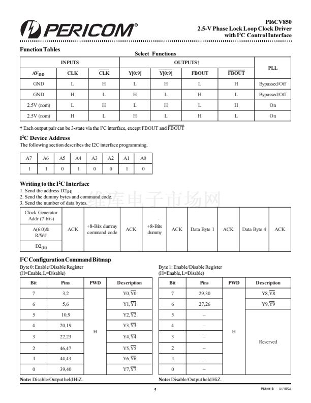
The device provides a standard mode (100kbits/s) I
2
C serial interface
for device control. Implementation is as a slave/receiver, and address
is specified in I
2
C device address table. Both I
2
C inputs (SDATA &
SCLK) provide integrated pullup resistors (typically 140 kohms) .
Two 8-bit I
2
C registers provide individual enable control for each
output pair. At powerup, all outputs default to enabled . Each pair can
be placed in a 3-state mode with a low-level output when a low-level
control bit is written to the control register. Registers must be accessed
in sequence (random access of the registers not supported).
For reduced EMI, the PI6CV850 also tracks Spread Spectrum
Clocking .
Since the PI6CV850 is based on PLL circuitry, it requires a stabili-
zation time to achieve phase-lock of the PLL. This stabilization time
is required following power up. Also required are changes to
various I
2
C controls that effect the PLL.
Y0
Y0
Y1
Y1
Block Diagram
SCLK
SDATA
AVDD
Test and
Logic
3
2
5
6
10
9
20
19
22
23
46
47
44
43
39
40
29
Pin Configuration
GND
1
2
3
4
5
6
7
8
9
10
11
12
13
14
15
16
17
18
19
20
21
22
23
24
48
47
46
45
44
43
42
41
40
GND
Y5
Y5
VDDQ
Y6
Y6
GND
GND
Y7
Y7
VDDQ
SDATA
FBIN
FBIN
VDDQ
FBOUT
FBOUT
GND
Y8
Y8
VDDQ
Y9
Y9
GND
Y0
Y0
VDDQ
Y1
Y1
GND
GND
Y2
Y2
VDDQ
SCLK
CLK
CLK
VDDI2C
AVDD
AGND
GND
Y3
Y3
Y2
Y2
Y3
Y3
Y4
Y4
Y5
Y5
Y6
Y6
Y7
Y7
Y8
Y8
48-Pin
A
39
38
37
36
35
34
33
32
31
30
29
28
27
26
25
CLK
CLK
FBIN
FBIN
13
14
36
35
30
PLL
27
26
Y9
Y9
VDDQ
Y4
Y4
GND
32 FBOUT
33 FBOUT
1
PS8481B
01/15/02


 1
1
 2
2
 3
3
 4
4
 5
5
 6
6
 7
7
