Powered by ICminer.com Electronic-Library Service CopyRight 2003
21098765432121098765432109876543210987654321210987654321098765432109876543212109876543210987654321098765432121098765432109876543210987654321
21098765432121098765432109876543210987654321210987654321098765432109876543212109876543210987654321098765432121098765432109876543210987654321
PI6C673F
133 MHz Single Chip Mobile Clock
Supports 440 BX
TM
/VIAPromedia
TM
Chipset
with Pentium II
TM
/Pentium III
TM
/Celeron
TM
Description
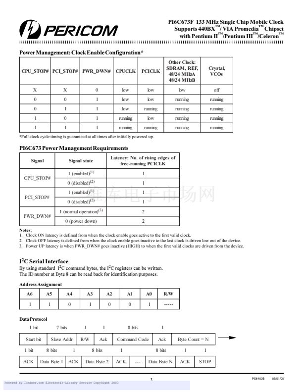
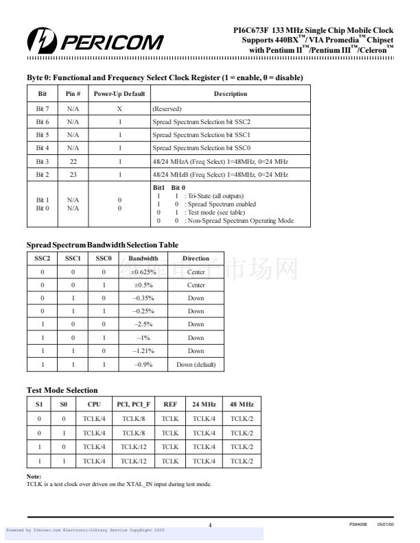
PI6C673F is the ideal low-cost solution for the 66/100/133 MHz
SDRAM-based mobile/handheld platform. It integrates high-speed,
low-noise, low-jitter, and low-skew clock generator and SDRAM
buffers. The device supports either discrete or modular processors,
three SO DIMMs, two 48/24 MHz outputs for USB and Super I/O, and
a combination of six PCI slots and devices. Power management
controls are realized with standard control signals such as:
PWR_DWN#, CPU_STOP#, and PCI_STOP#. To further reduce
power consumption and to minimize EMI emission, each individual
output can be enabled/disabled through I
2
C interface.
A wide range of SSC (Spread Spectrum Clock) options allow users
to choose the best mode for minimal EMI. Generous power supply
pins ensure that the device will have low noise and high performance.
Features
聲 Integrated clock and buffer for Pentium II
聶
/Pentium III
聶
/
Celeron
聶
processors
聲 I
2
C: 2-Wire Serial Interface. Device vendor ID is readable
聲 Edge rate control of clock output signals for EMI suppression
聲 Eight Spread Spectrum options for optimal EMI suppression
聲 Individual clock output enable/disable
聲 Two CPUCLKs, with enhanced drive
聲 Seven PCI clocks
聲 Seven SDRAM clocks for 3 SO DIMMs.
聲 Three 14.31818 MHz clocks
(REF2 has an enhanced output drive)
聲 Two 48/24 MHz clocks
聲 Low skew and low power consumption.
聲 Extended temperature range 0擄C - 85擄C
聲 Package: 48-pin 240 mil TSSOP (A)
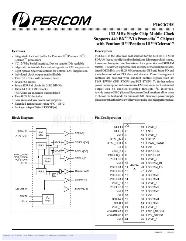
Block Diagram
Pin Configuration
REF1
REF0
Vss
XTAL_IN
XTAL_OUT
S1
Vddq_3
PCICLK_F
PCICLK0
Vss
PCICLK1
PCICLK2
PCICLK3
PCICLK4
Vddq_3
PCICLK5
Vss
S0
SDATA
SCLK
Vddq_3
48/24MHzA
48/24MHzB
Vss
48
1
47
2
46
3
45
4
44
5
43
6
42
7
41
8
40
9
39
10
48-Pin
38
11
A
37
12
13
36
14
35
15
34
16
33
17
32
18
31
19
30
20
29
21
28
22
27
23
26
25
24
Vddq_3
N/C
Vddq_3
REF2
PWR_DWN#
Vss
CPUCLK0
CPUCLK1
Vddq_2
SDRAM_IN
SDRAM_FB
Vss
SDRAM0
SDRAM1
Vddq_3
SDRAM2
SDRAM3
Vss
SDRAM4
SDRAM5
Vddq_3
CPU_STOP#
PCI_STOP#
Vddq_3
XTAL_IN
XTAL_OUT
Xtal
OSC
PLL1
STOP
STOP
Control
Logic
PLL2
REF[0-2]
CPUCLK[0-1]
PCICLK[0-5]
PCICLK_F
48/24MHzA/B
SDRAM_FB
PWR_DWN#
CPU_STOP#
PCI_STOP#
S1, S0
/2
SDRAM_IN
SDATA
SCLK
I2C
Logic
SDRAM[0-5]
1
PS8400B
05/01/00


 1
1
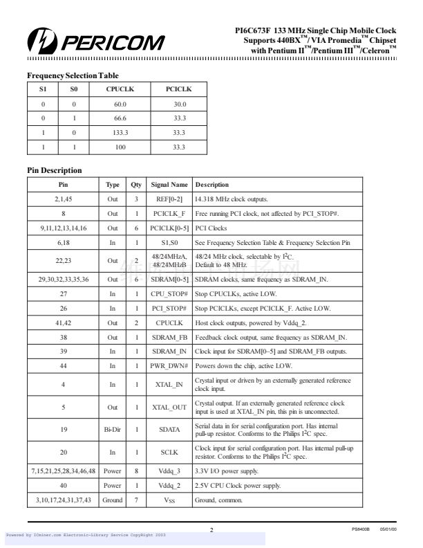 2
2
 3
3
 4
4
 5
5
 6
6
 7
7
 8
8
 9
9
 10
10
