-
-

- 手機(jī)版
-

- 芯視頻 APP
-

- 微信公眾號(hào)
-

- 維庫官方抖音
-

- 微信頭條號(hào)
-
- |
- |
- |
- |

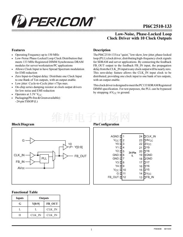
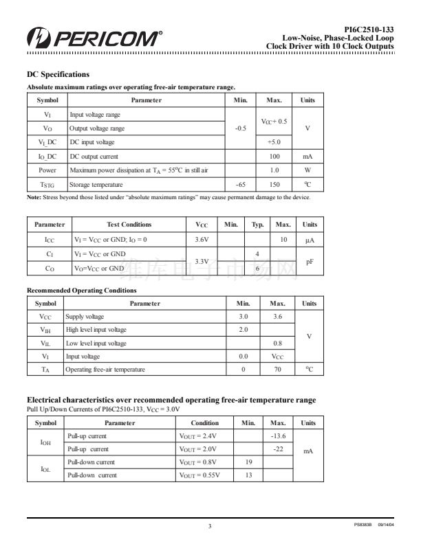
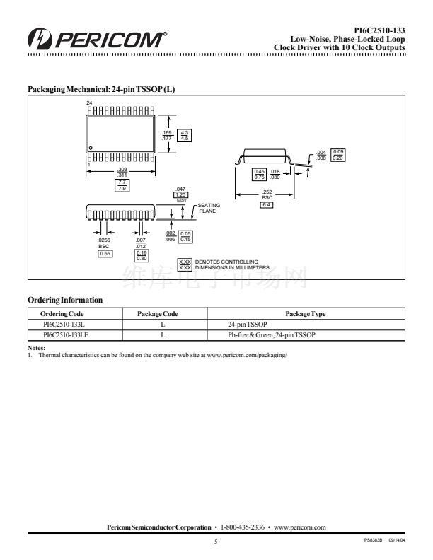
PI6C2510-133
Low-Noise, Phase-Locked Loop Clock Driver with 10 Clock Outp...
142.55KB
5頁
![]() PERICOM
PERICOM
掃碼查看芯片數(shù)據(jù)手冊
上傳產(chǎn)品規(guī)格書


聯(lián)系人:
聯(lián)系方式:

 1
1
 2
2
 3
3
 4
4
 5
5
