鈥?/div>
Operating Frequency up to 150 MHz
Low-Noise Phase-Locked Loop Clock Distribution that
meets 133 MHz Registered DIMM Synchronous DRAM
modules for server/workstation/PC applications
Allows Clock Input to have Spread Spectrum modulation
for EMI reduction
Zero Input-to-Output delay: Distribute one Clock Input
to one Bank of Ten outputs, with an output enable.
Low jitter: Cycle-to-Cycle jitter 鹵75ps max.
On-chip series damping resistor at clock output drivers
for low noise and EMI reduction
Operates at 3.3V V
CC
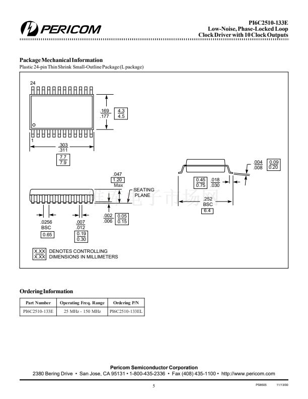
Package: Plastic 24-pin TSSOP (L)
Logic Block Diagram
Product Pin Configuration
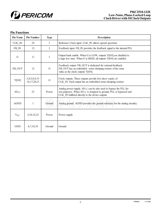
G
10
Y[0:9]
FB_OUT
CLK_IN
FB_IN
AVcc
PLL
AGND
V
CC
Y0
Y1
Y2
GND
GND
Y3
Y4
V
CC
G
FB_OUT
1
2
3
4
5
6
7
8
9
10
11
12
24-Pin
L
24
23
22
21
20
19
18
17
16
15
14
13
CLK_IN
AV
CC
V
CC
Y9
Y8
GND
GND
Y7
Y6
Y5
V
CC
FB_IN�
Functional Table
Inputs
G
L
H
Outputs
Y[0:9]
L
CLK_IN
FB_OUT
CLK_IN
CLK_IN
1
PS8505
11/13/00


 1
1
 2
2
 3
3
 4
4
 5
5
