音影先锋亚洲天堂网|电影世界尽头的爱完整版播放|国产 熟女 91|高清无码免费观看欧美日韩|韩国一区二区三区黄色录像|美女亚洲加勒比在线|亚洲综合网 开心五月|7x成人在线入口|成人网站免费日韩毛片区|国产黄片?一级?二级?三级

PI6C2501 Datasheet

  • PI6C2501

  • Clock IC | 25 to 80 MHz. 1 Output Zero-Delay Clock Driver

  • 4頁

  • ETC

掃碼查看芯片數(shù)據(jù)手冊

上傳產(chǎn)品規(guī)格書

PDF預覽

V
21098765432121098765432109876543210987654321210987654321098765432109876543212109876543210987654321098765432121098765432109876543210987654321
21098765432121098765432109876543210987654321210987654321098765432109876543212109876543210987654321098765432121098765432109876543210987654321
PI6C2501
Phase-Locked Loop Clock Driver
Product Features
鈥?/div>
High-Performance, Phase-Locked-Loop Clock Distribution
鈥?/div>
Allows Clock Input to have Spread Spectrum modulation
for EMI reduction
鈥?/div>
Zero Input-to-Output delay
鈥?/div>
Low jitter: Cycle-to-Cycle jitter 鹵100ps max.
鈥?/div>
On-chip series damping resistor at clock output drivers
for low noise and EMI reduction
鈥?/div>
Operates at 3.3V V
CC
鈥?/div>
Wide range of Clock Frequencies up to 80 MHz
鈥?/div>
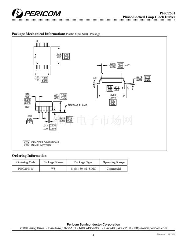
Package: Plastic 8-pin SOIC (W)
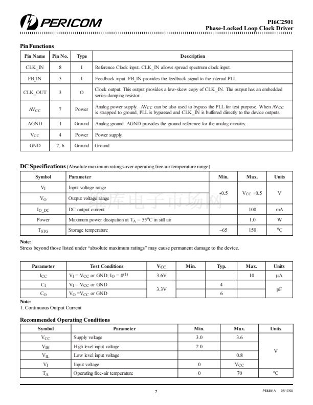
Product Description
The PI6C2501 features a low-skew, low-jitter, phase-locked loop
(PLL) clock driver. By connecting the CLK_OUT output to the
feedback FB_IN input, the propagation delay from the CLK_IN
input to CLK_OUT output will be nearly zero.
Application
If a system designer needs more than 16 outputs with the features
just described, using two or more zero-delay buffers, such as the
PI6C2509Q, or PI6C2510Q, is likely to be impractical. The
device-to-device skew introduced can significantly reduce the
performance. Pericom recommends using a zero-delay buffer and
an eighteen output non-zero-delay buffer. As shown in Figure 1,
this combination produces a zero-delay buffer with all the signal
characteristics of the original zero-delay buffer, but with as many
outputs as the non-zero-delay buffer part. For example, when
combined with an eighteen output non-zero delay buffer, a system
designer can create a seventeen-output zero-delay buffer.
Logic Block Diagram
Product Pin Configuration
AGND
GND
CLK_OUT
VCC
1
2
3
4
8
CLK_IN
AVCC
GND
FB_IN
CLK_IN
PLL
FB_IN
AV
CC
CLK_OUT
8-Pin
W
7
6
5
Feedback
C
Reference
Clock
Signal
Zero Delay
Buffer
PI6C2501
CLK_OUT
18 Outputs
Non-PLL
Buffer
17
Figure 1. This Combination Provides Zero-Delay Between
the Reference Clock Signal and 17 Outputs
1
PS8381A
07/17/00

PI6C2501相關型號PDF文件下載

  • 型號
    版本
    描述
    廠商
    下載
  • 英文版
    Clock IC | 100 MHz Dual Pentium II Desktop Clock
    ETC
  • 英文版
    Clock IC | 100 MHz Dual Pentium II Desktop Clock
  • 英文版
    Precision Clock Synthesizer for Mobile PCs
    PERICOM
  • 英文版
    Precision Clock Synthesizer for Mobile PCs
    PERICOM [P...
  • 英文版
    Precision Clock Synthesizer
    PERICOM
  • 英文版
    Precision Clock Synthesizer
    PERICOM [P...
  • 英文版
    Spread Spectrum Clock Synthesizer for Desktop Pentium II
    PERICOM
  • 英文版
    Spread Spectrum Clock Synthesizer for Desktop Pentium II
    PERICOM [P...
  • 英文版
    Precision Clock Synthesizer for Mobile PCs
    Pericom Semicon...
  • 英文版
    Pentium/Pro System Clock Chip
    PERICOM
  • 英文版
    Pentium/Pro System Clock Chip
    PERICOM [P...
  • 英文版
    Clock IC | Desktop PC. 18 Output Clock Driver
    ETC
  • 英文版
    Clock IC | Desktop PC. 18 Output Clock Driver
  • 英文版
    Clock IC | Mobile PC. 10 Output Clock Driver
    ETC
  • 英文版
    Clock IC | Desktop PC. 13 Output Clock Driver (IMI compatibl...
    ETC
  • 英文版
    3.3V PRECISION CLOCK GENERATOR
    PERICOM
  • 英文版
    3.3V PRECISION CLOCK GENERATOR
    PERICOM [P...
  • 英文版
    3.3V PRECISION CLOCK GENERATOR
    PERICOM
  • 英文版
    3.3V PRECISION CLOCK GENERATOR
    PERICOM [P...
  • 英文版
    Clock IC | 750ps Accuracy. 5V. TTL. 3.75 to 80 MHz
    ETC

掃碼下載APP,
一鍵連接廣大的電子世界。

在線人工客服

買家服務:
賣家服務:
技術客服:

0571-85317607

網(wǎng)站技術支持

13606545031

客服在線時間周一至周五
9:00-17:30

關注官方微信號,
第一時間獲取資訊。

建議反饋

聯(lián)系人:

聯(lián)系方式:

按住滑塊,拖拽到最右邊
>>
感謝您向阿庫提出的寶貴意見,您的參與是維庫提升服務的動力!意見一經(jīng)采納,將有感恩紅包奉上哦!