鈥?/div>
Maximum Operating Frequency: 133MHz
Low skew < 350ps
Low propagation delay < 3.5ns
Fast output rise/fall time < 1.0ns
Balanced CMOS outputs
Industrial Operation: -40
0
C to +85
0
C
3.3V supply voltage
5V tolerant input
Available in 28-pin 50mil PLCC
Description
The P6C1816 is designed by CMOS technology to achieve fast
speed, low skew, low propagation delay and fast rise and fall time
for applications requiring large fanouts, like datacom, telecom
and network systems.
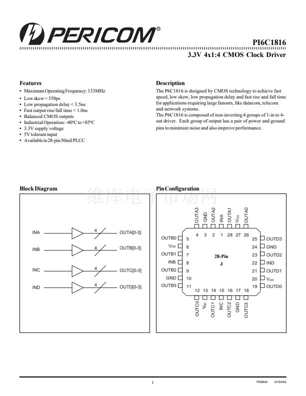
The P6C1816 is composed of non-inverting 4 groups of 1-in to 4-
out driver. Each group of output has a pair of power and ground
pins to minimize noise and also improve performance.
Block Diagram
Pin Configuration
OUTD3
GND
OUTD2
IND
OUTD1
V
DD
OUTD0
INB
4
OUTB[0-3]
V
DD
OUTB1
INB
28-Pin
J
23
22
21
20
19
INC
4
OUTC[0-3]
OUTB2
GND
IND
4
OUTD[0-3]
OUTB3
12 13 14 15 16 17 18
1
PS8624
07/24/02


 1
1
 2
2
 3
3
 4
4
