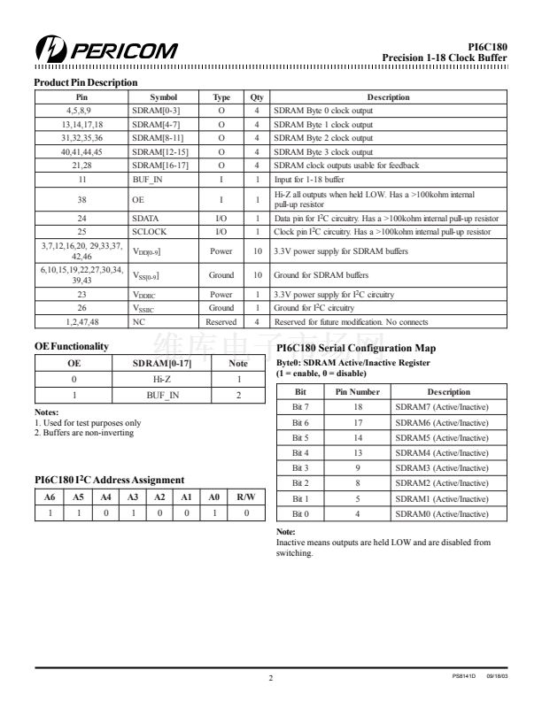
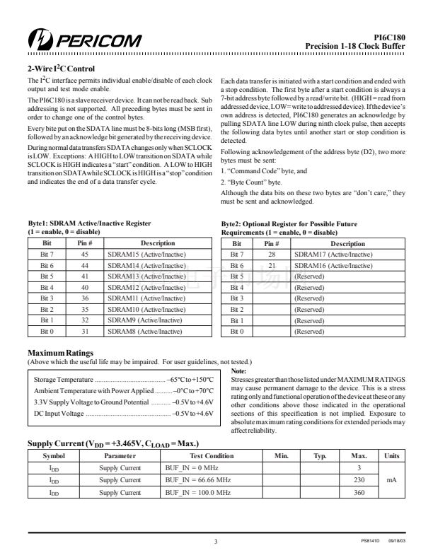
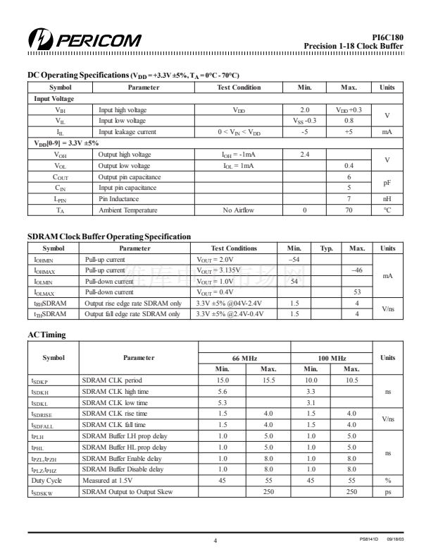
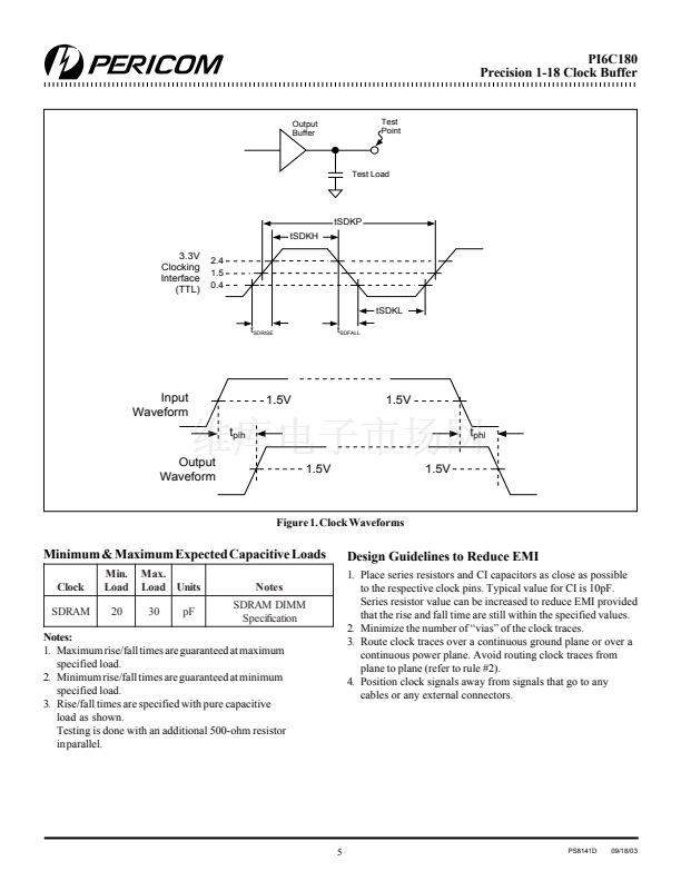
鈥?/div>
48-pin SSOP package (V)
Description
The PI6C180, a high-speed low-noise 1-18 non-inverting buffer
designed for SDRAM clock buffer applications operates up to 100
MHz.
At power up all SDRAM output are enabled and active. The I
2
C
Serial control may be used to individually activate/deactivate any
of the 18 output drivers.
The output enable (OE) pin may be pulled low to put all outputs in a
Hi-Z state.
Note:
Purchase of I
2
C components from Pericom conveys a license to
use them in an I
2
C system as defined by Philips.
Logic Block Diagram
Product Pin Configuration
NC
1
2
3
4
5
6
7
8
9
10
48-Pin
11
12
13
14
15
16
17
18
19
20
21
22
23
24
48
47
46
45
44
43
42
41
40
39
38
37
36
35
34
33
32
31
30
29
28
27
26
25
NC
NC
V
DD9
SDRAM15
SDRAM14
V
SS9
V
DD8
SDRAM13
SDRAM12
V
SS8
OE
V
DD7
SDRAM11
SDRAM10
V
SS7
V
DD6
SDRAM9
SDRAM8
V
SS6
V
DD5
SDRAM17
V
SS5
V
SS
IIC
SCLOCK
SDRAM0
NC
V
DD0
SDRAM0
SDRAM1
V
SS0
V
DD1
SDRAM2
SDRAM3
V
SS1
BUF_IN
V
DD2
SDRAM4
SDRAM5
V
SS2
V
DD3
SDRAM6
SDRAM7
V
SS3
V
DD4
SDRAM16
V
SS4
V
DD
IIC
SDATA
SDRAM1
BUF_IN
SDRAM2
SDRAM3
V
SDRAM17
OE
SDATA
SCLOCK
I2C
I/O
1
PS8141D
09/18/03


 1
1
 2
2
 3
3
 4
4
 5
5
 6
6
 7
7
