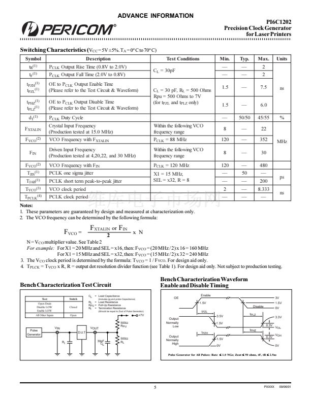
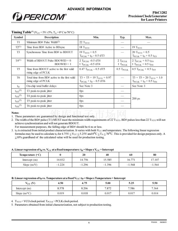
ADVANCE INFORMATION
21098765432121098765432109876543210987654321210987654321098765432109876543212109876543210987654321098765432121098765432109876543210987654321
21098765432121098765432109876543210987654321210987654321098765432109876543212109876543210987654321098765432121098765432109876543210987654321
PI6C1202
Precision Clock Generator
for Laser Printers
Features
聲
Supports laser printer pixel rates up to 120 MHz.
聲
Jitter less than 200ps.
聲
Easily programmable frequency selections via parallel
interface. Post divider (R) designed to load only during
the Beam Detect interval.
聲
Source clock input can be from crystal or oscillator.
聲
Crystal frequency range from 8 MHz to 22 MHz.
聲
Oscillator frequency range from 8 MHz to 30 MHz.
聲
Active LOW asynchronous reset input for synchronization
with engine via Beam Detect Input.
聲
Synchronized Beam Detect Output to support external state
machines.
聲
Glitch-less clock output after Beam Detect.
聲
Supports dynamic frequency changes on a line-per-line basis.
聲
Mixed line resolution supports half-toning and gray scale
operations.
聲
Minimizes controller memory utilization (low-resolution text
mixed with high-resolution images).
聲
On-chip VCO loop filter (no external components).
聲
On-chip crystal oscillator (modified Pierce).
聲
Single 5V power supply.
聲
Low power consumption.
聲
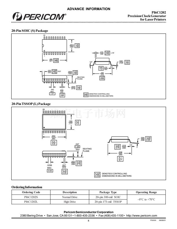
Packaging:
20-pin wide body SOIC (S), 20-pin wide body TSSOP (L)
Description
The PI6C1202 is an advanced CMOS clock generator designed
specifically to support pixel clock generation in low-cost laser
printers. Capable of generating highly stable clock frequencies up
to 120 MHz, this device supports printer engines with dot resolu-
tions of 1,200 dpi and above. Page speeds may range from 4 pages
per minute to better than 60 pages per minute.
Mixed-line resolution supports half-toning and gray scale opera-
tions (low-resolution text mixed with high-resolution images) and
minimizes controller memory utilization.
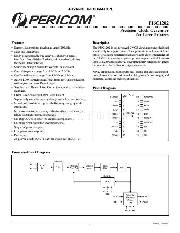
Pinout Diagram
X1/ICLK
X2
SEL0
GND
SEL1
SEL2
VCC
AGND
OE
AVCC
1
2
3
4
5
6
7
8
9
10
20
19
18
17
BDOWID
GND
PCLK
GND
BD#
BDOUT
BDOPOL
R0
R1
R2
20-Pin
L, S
16
15
14
13
12
11
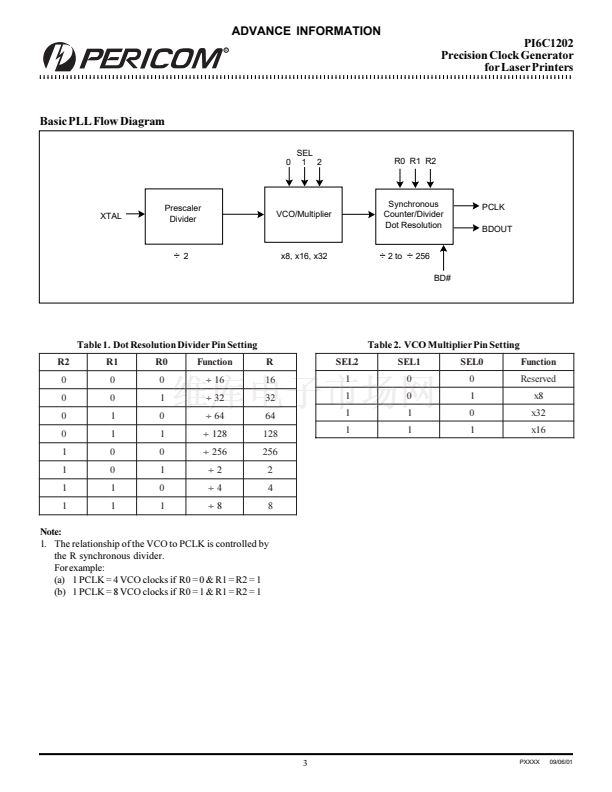
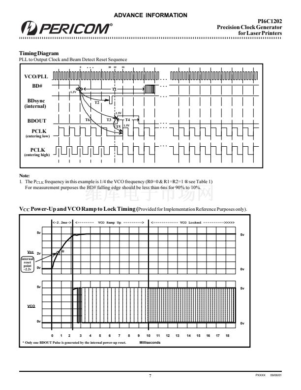
Functional Block Diagram
Prescale
X1
X2
CLK
IN
.
. 2
Phase &
Freq Det
Charge
Pump
Loop
Filter
VCO
Multiplier
.
. N
0
1 2
SEL
BD#
OE
Control &
Resolution
Select
(R)
BDOUT
PCLK
R0 R1 R2
1
PXXXX
09/06/01


 1
1
 2
2
 3
3
 4
4
 5
5
 6
6
 7
7
 8
8
