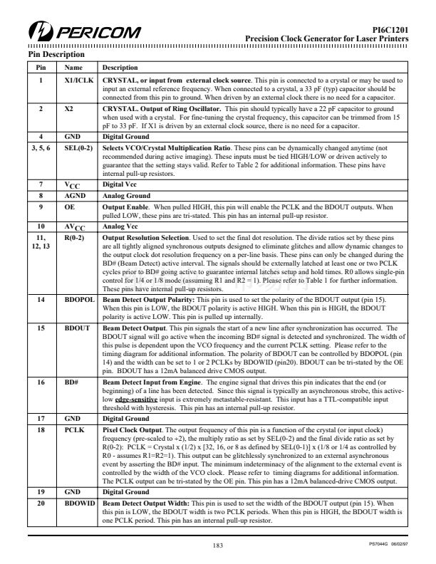
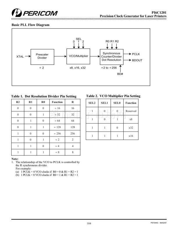
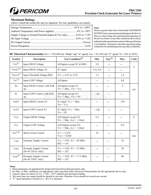
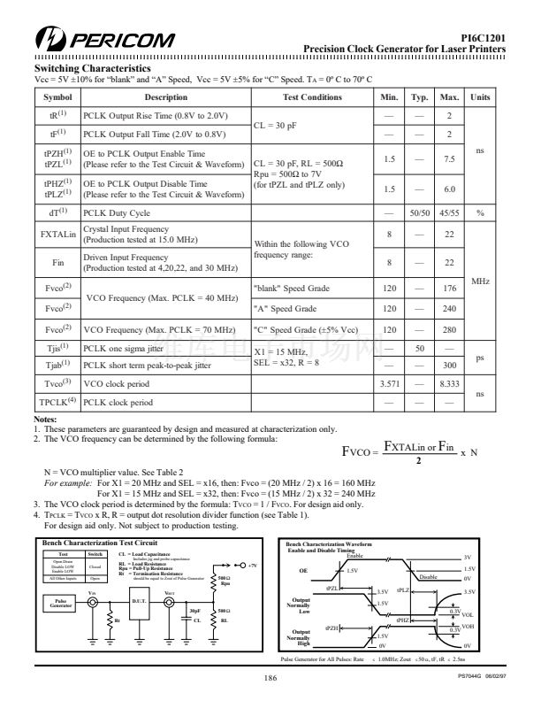
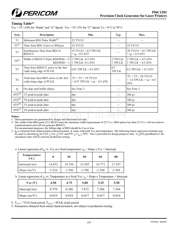
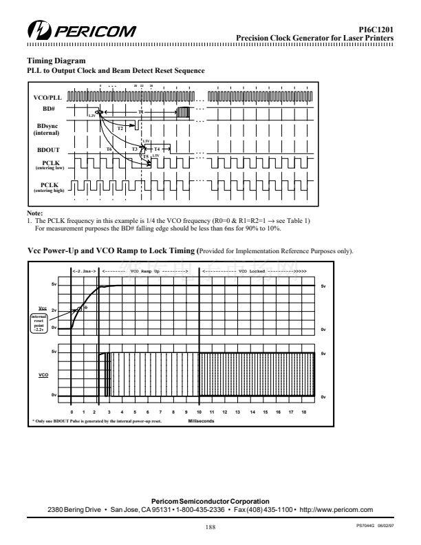
PI6C1201
21098765432121098765432109876543210987654321210987654321098765432109876543212109876543210987654321098765432121098765432109876543210987654321
21098765432121098765432109876543210987654321210987654321098765432109876543212109876543210987654321098765432121098765432109876543210987654321
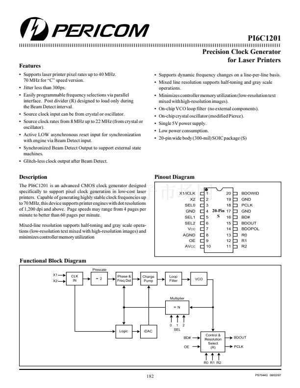
Features
聲
Supports laser printer pixel rates up to 40 MHz.
70 MHz for 聯(lián)C聰 speed version.
聲
Jitter less than 300ps.
聲
Easily programmable frequency selections via parallel
interface. Post divider (R) designed to load only during
the Beam Detect interval.
聲
Source clock input can be from crystal or oscillator.
聲
Source clock rates from 8 MHz up to 22 MHz (from crystal or
oscillator).
聲
Active LOW asynchronous reset input for synchronization
with engine via Beam Detect input.
聲
Synchronized Beam Detect Output to support external state
machines.
聲
Glitch-less clock output after Beam Detect.
Precision Clock Generator
for Laser Printers
聲
Supports dynamic frequency changes on a line-per-line basis.
聲
Mixed line resolution supports half-toning and gray scale
operations.
聲
Minimizes controller memory utilization (low-resolution text
mixed with high-resolution images).
聲
On-chip VCO loop filter (no external components).
聲
On-chip crystal oscillator (modified Pierce).
聲
Single 5V power supply.
聲
Low power consumption.
聲
20-pin wide body (300-mil) SOIC package (S)
Description
The PI6C1201 is an advanced CMOS clock generator designed
specifically to support pixel clock generation in low-cost laser
printers. Capable of generating highly stable clock frequencies up
to 70 MHz, this device supports printer engines with dot resolutions
of 1,200 dpi and above. Page speeds may range from 4 pages per
minute to better than 60 pages per minute.
Mixed-line resolution supports half-toning and gray scale opera-
tions (low-resolution text mixed with high-resolution images) and
minimizes controller memory utilization
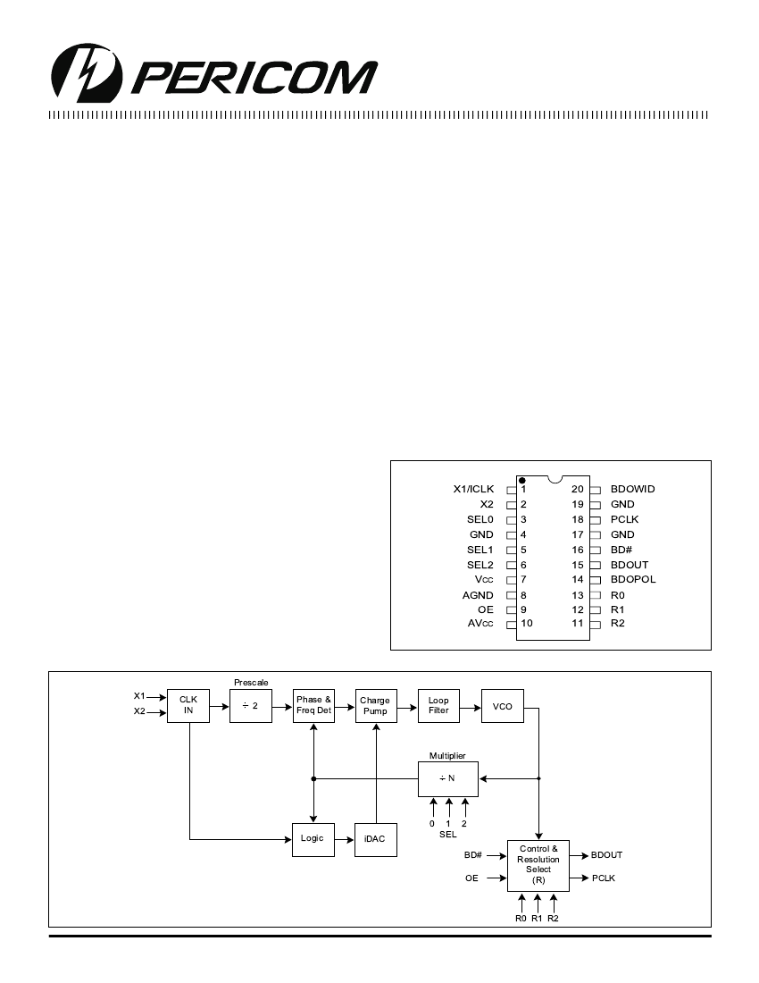
Pinout Diagram
X1/ICLK
X2
SEL0
GND
SEL1
SEL2
V
CC
AGND
OE
AV
CC
1
20
2
19
3
18
4
20-Pin
17
S
16
5
6
15
7
14
8
13
9
12
10
11
BDOWID
GND
PCLK
GND
BD#
BDOUT
BDOPOL
R0
R1
R2
Functional Block Diagram
Prescale
X1
X2
CLK
IN
.
. 2
Phase &
Freq Det
Charge
Pump
Loop
Filter
VCO
Multiplier
.
. N
0
Logic
iDAC
1 2
SEL
BD#
OE
Control &
Resolution
Select
(R)
BDOUT
PCLK
R0 R1 R2
PS7044G 06/02/97
182


 1
1
 2
2
 3
3
 4
4
 5
5
 6
6
 7
7
