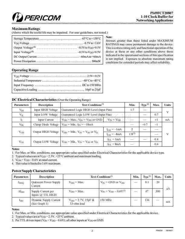
21098765432121098765432109876543210987654321210987654321098765432109876543212109876543210987654321098765432121098765432109876543210987654321
21098765432121098765432109876543210987654321210987654321098765432109876543212109876543210987654321098765432121098765432109876543210987654321
21098765432121098765432109876543210987654321210987654321098765432109876543212109876543210987654321098765432121098765432109876543210987654321
PI49FCT20807
1-10 Clock Buffer for
Networking Applications
Product Features
聲 High Frequency >150 MHz
聲 High-speed, low-noise, non-inverting 1-10 buffer
聲 Low-skew (<150ps) between any two output clocks
聲 Low duty cycle distortion <300ps
聲 Low propagation delay <3.5ns
聲 Multiple V
DD
, GND pins for noise reduction
聲 2.5V supply voltage
聲 Available in SOIC, SSOP, and QSOP packages
Description
The PI49FCT20807, a 2.5V compatible, high-speed, low-noise 1-10
non-inverting clock buffer, is designed to target networking appli-
cations that require low-skew, low-jitter, and high-frequency clock
distribution. Providing output-to-output skew as low as 150ps, the
PI49FCT20807 is an ideal clock distribution device for synchronous
systems. Designing synchronous networking systems requires a
tight level of skew from a large number of outputs.
Product Pin Description
Pin Name
BUF_IN
CLK [0:9]
GND
V
DD
Input
O utputs
Ground
Power
D e s cription
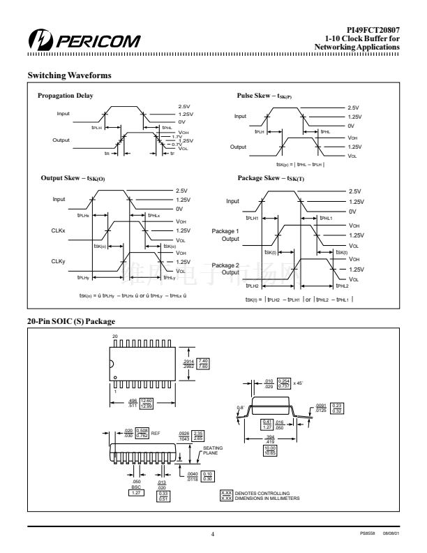
Block Diagram
CLK0
Pin Configuration
BUF_IN
GND
1
2
3
4
5
6
7
8
9
10
20
19
18
VDD
CLK9
CLK8
GND
CLK7
VDD
CLK6
GND
CLK5
CLK4
CLK1
BUF_IN
CLK2
CLK0
VDD
CLK1
GND
CLK2
20-Pin
H, Q, S
17
16
15
14
13
12
11
CLK3
VDD
CLK3
GND
CLK9
1
PS8558
08/08/01


 1
1
 2
2
 3
3
 4
4
 5
5
